· Thomas Webb · News · 7 min read
AT&S Invests EUR2 Billion in Malaysia AI
Austrian IC substrate manufacturer AT&S announces EUR2 billion investment to expand Kulim, Malaysia facility for AI chip packaging. Backed by AMD and Intel commitments, this expansion addresses the global AI substrate bottleneck and signals continued tightening of advanced packaging capacity through 2028.
Quick Answer
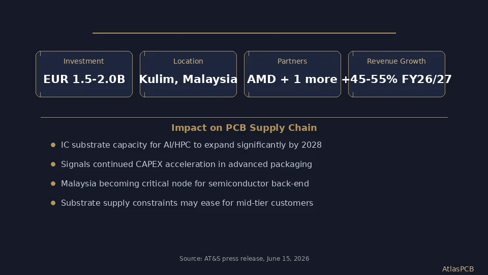
AT&S has announced a EUR2 billion (US$2.3 billion) investment to fully expand its IC substrate manufacturing facility in Kulim, Malaysia, backed by long-term commitments from AMD and Intel. The expansion will bring online a previously unused building and expand the existing Kulim plant, specifically targeting high-end AI chip substrates used in advanced GPU and accelerator packaging. AT&S simultaneously raised its 2026/27 revenue growth forecast to 45-55%, and its stock surged 30% to a record EUR200. This signals that AI substrate demand continues to outpace supply, with implications for lead times and pricing across the broader PCB and substrate ecosystem.
EUR2 Billion Bet on AI Substrate Demand
Austria-headquartered AT&S — one of the world’s leading IC substrate manufacturers — announced on June 15, 2026 that it will invest up to EUR2 billion (approximately US$2.3 billion) to expand its advanced substrate manufacturing capacity at its Kulim, Malaysia site. The investment is fully funded and backed by long-term customer commitments from AMD and Intel, two of the largest consumers of AI accelerator packaging.
The announcement sent AT&S shares surging nearly 30% to a record high of EUR200 in European trading, reflecting investor confidence that the AI infrastructure buildout continues to accelerate rather than plateau. CEO Michael Mertin confirmed to Reuters that the company will “fully expand” the Kulim site, including fitting out a previously unused building at a second location within the Kulim industrial zone.
AT&S simultaneously raised its 2026/27 fiscal year revenue growth forecast from a previous range to 45-55% year-over-year growth — a remarkable figure for a company already operating at scale. This upgrade signals that customer demand visibility extends well beyond typical order horizons, suggesting multi-year AI hardware procurement commitments from hyperscalers.
Why AI Needs Massive Substrate Capacity
The substrate shortage affecting AI chip production is not new — it has been building since 2023 when the first wave of large-language-model training demand overwhelmed existing packaging capacity. What makes the current phase different is the shift from GPU-only demand to a broad-based need across inference accelerators, custom ASICs, and networking silicon.
Modern AI accelerators like AMD’s Instinct MI series and Intel’s Gaudi processors require exceptionally large packaging substrates. A single high-end AI GPU package can consume a substrate measuring 70x70mm or larger, with dozens of redistribution layers at sub-10um resolution. The manufacturing complexity is comparable to advanced semiconductor fabrication itself, requiring clean-room environments, photolithography equipment, and multi-month qualification cycles.
The Kulim expansion specifically targets this high-end segment. Unlike standard PCB fabrication where capacity can be added incrementally with additional production lines, IC substrate manufacturing requires massive upfront capital investment in specialized equipment — ABF lamination presses, advanced laser drilling systems with submicron positioning, and ultra-precision plating lines. The EUR2 billion investment scale reflects this capital intensity.
AI HARDWARE PCB EXPERTISE
Building the Motherboard That Receives AI Accelerators
While AT&S makes the substrate inside the package, AtlasPCB fabricates the high-layer-count motherboards and backplanes that these AI modules plug into. Up to 30 layers with controlled impedance for PCIe Gen 5/6 routing.
Get AI Server PCB Quote ›
Supply Chain Implications for PCB Designers
The AT&S expansion is one data point in a broader pattern of investment flowing into AI packaging infrastructure. In the past 12 months, we have seen Nan Ya PCB, Samsung Electro-Mechanics, Ibiden, and Shinko all announce significant substrate capacity expansions. The collective message is clear: the industry expects AI hardware demand to grow faster than supply through at least 2028.
For hardware engineers designing AI server motherboards, GPU baseboard PCBs, and high-performance computing platforms, this has several practical implications:
Material availability pressure continues. ABF (Ajinomoto Build-up Film) and other advanced build-up materials are consumed in higher volumes by substrate manufacturers, creating allocation competition with PCB fabricators who use similar materials for HDI construction. If your design uses ABF-based build-up layers, plan for longer material lead times.
BGA substrate integration complexity increases. As AI chip packages grow larger and more complex (multi-chiplet, 2.5D/3D integration), the PCB must accommodate larger BGA footprints, tighter ball pitch, and more demanding power delivery requirements. The mechanical stress from large packages on the PCB also increases, requiring careful attention to warpage control and underfill compatibility.
Power delivery demands escalate. Next-generation AI accelerators push toward 1000A+ current delivery through the motherboard PCB. This drives requirements for heavy copper layers, optimized power plane splits, and high-density decoupling capacitor placement — all of which increase PCB layer count and fabrication complexity.
What This Means for Your Next AI Hardware Design
If you are designing PCBs that interface with advanced AI accelerators, the AT&S expansion validates that the performance and complexity requirements will continue escalating. Design choices you make today should anticipate:
Higher layer counts for power delivery. Budget for 20-30 layer boards with dedicated power and ground plane pairs for each voltage rail. The days of routing AI accelerator power through 8-layer boards are ending as current requirements exceed what thin copper planes can handle without excessive voltage drop.
Low-loss laminates for high-speed interconnect. PCIe Gen 5 and Gen 6 signals connecting CPU to AI accelerator require material with Df below 0.005. Standard FR-4 cannot support the 32 GT/s+ data rates at useful trace lengths. Plan for hybrid stackups with low-loss material on signal layers and standard FR-4 on power layers to balance cost.
Thermal management integration. With AI packages dissipating 300-700W in a single socket, the PCB itself becomes part of the thermal path. Thermal vias under the package, copper coin inserts, and metal-core substrate regions are increasingly common design features that must be accounted for in fabrication planning.
HIGH-PERFORMANCE COMPUTING
Up to 30 Layers, Low-Loss Materials, Heavy Copper PDN
AtlasPCB fabricates the complex multilayer boards that AI server platforms demand. Megtron 6, controlled impedance, backdrilling, and up to 5oz copper for power delivery.
Industry Context: The Substrate Investment Wave
AT&S joins a growing list of companies racing to expand AI substrate and advanced packaging capacity:
| Company | Investment | Location | Target |
|---|---|---|---|
| AT&S | EUR2.0B | Malaysia (Kulim) | IC substrates for AMD/Intel |
| Nan Ya PCB | ~US$2B | Taiwan, Thailand | ABF substrates |
| Samsung E-M | ~US$1.5B | Korea, Vietnam | FC-BGA substrates |
| Ibiden | ~US$1.8B | Japan, Malaysia | High-end IC substrates |
| TSMC (CoWoS) | US$5B+ | Taiwan, Japan | Advanced packaging |
The collective investment exceeding US$12 billion in substrate and advanced packaging capacity over 2025-2028 represents an industry consensus: AI hardware demand is structural, not cyclical. Unlike previous semiconductor cycles where overinvestment led to price crashes, the substrate segment has such extended qualification timelines (12-18 months for new capacity to reach volume production) that even aggressive investment today will barely meet projected 2028 demand.
For PCB designers and hardware engineers, the strategic takeaway is to plan for continued cost pressure on advanced materials and extended lead times for complex fabrication. Building strong fabrication partnerships with suppliers who have material allocation strategies becomes a competitive advantage.
ATLASPCB
Secure Your Material Allocation for AI Hardware PCBs
With substrate materials tightening, early engagement with your PCB fabricator matters. Lock in material availability and lead time commitments for your next AI platform build.
Start Your Quote ›
Related Reading:
About AtlasPCB — We specialize in complex PCB manufacturing for HDI, RF, and high-reliability applications. Explore our impedance-controlled PCB manufacturing . Every order includes free engineering review. Get your quote.
Reviewed by AtlasPCB Engineering Team — IPC-certified manufacturing specialists with 15+ years of production experience in HDI, RF, and high-reliability PCB fabrication. Content based on factory floor data and real customer design reviews.
Frequently Asked Questions
What does AT&S manufacture in Malaysia?
How does the AT&S expansion affect PCB fabrication lead times?
What is the difference between IC substrates and PCBs?
- AT&S
- IC substrate
- AI packaging
- Malaysia
- PCB industry news
- advanced packaging
- semiconductor