· Thomas Webb · Engineering · 6 min read
AI-Driven PCB Substrate Demand
Taiwanese substrate maker Kinsus reports AI-driven demand for ABF and BT substrates has extended order visibility to 2028-2029, as CoWoS packaging, 2nm chips, and agentic AI drive unprecedented capacity expansion. Analysis of what this means for PCB manufacturers and hardware engineers.
Quick Answer
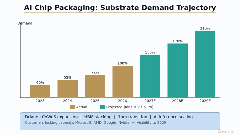
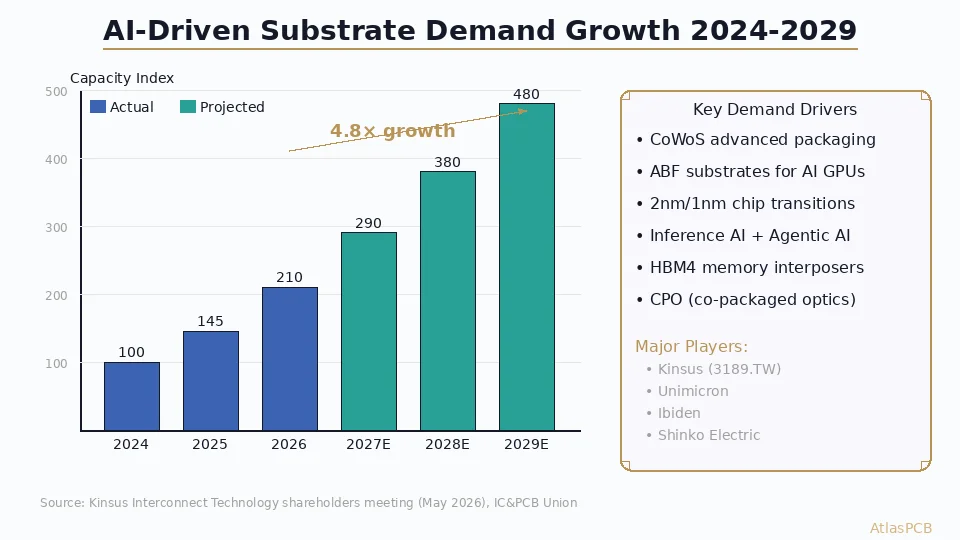
Kinsus Interconnect Technology, a leading Taiwanese PCB substrate manufacturer, reported at its May 2026 shareholders meeting that AI-driven demand has extended substrate order visibility and capacity planning into 2028 and 2029 — far beyond normal 6-12 month lead times. Their ABF substrate business has surpassed its 2022 peak, driven by the semiconductor industry's transition to 2nm/1nm processes and surging CoWoS advanced packaging demand. The company is adopting a technology-node-focused expansion strategy rather than broad capacity buildouts, targeting next-generation packaging and chip interconnect technologies.
The AI Substrate Supercycle
At its annual shareholders meeting in May 2026, Taiwanese PCB substrate manufacturer Kinsus Interconnect Technology Corp. (3189.TW) delivered a message that sent ripples through the electronics supply chain: AI-driven demand has extended their substrate order visibility and expansion planning into 2028 and 2029 — an unprecedented planning horizon for an industry accustomed to 6-12 month order cycles.
This isn’t corporate optimism. It reflects a structural transformation in semiconductor packaging that directly impacts every level of the PCB supply chain, from advanced substrates down to standard server motherboards.
What Kinsus Reported: Key Findings
ABF Substrate Demand Surpasses 2022 Peak
Kinsus President and CEO Chen Ho-Hsu confirmed that the company’s ABF substrate business has already exceeded its previous peak in 2022 — the year that saw cryptocurrency mining and pandemic-era computing demand drive record substrate orders. The current surge is different: it’s being driven by genuine AI infrastructure buildout rather than speculative demand.
Technology-Node-Focused Expansion
Rather than pursuing broad capacity buildouts (which risk overcapacity if demand softens), Kinsus is adopting a “technology node” expansion strategy. This means:
- Targeted investment in manufacturing for next-generation packaging (CoWoS-L, CoWoS-R, and future InFO variants)
- Process qualification for 2nm and 1nm chip interconnect requirements
- Equipment upgrades focused on finer line/space capability (sub-10μm L/S)
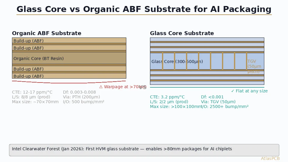
- Panel size expansion for larger AI chip interposers (>100mm × 100mm)
Customer Capacity Lock-In
Multiple data points confirm that major AI chip companies have locked in substrate capacity through 2029:
- Microsoft, AMD, and Google continue actively securing capacity from Taiwan’s substrate supply chain
- NVIDIA reportedly committed to multi-year ABF substrate agreements with Ibiden and Unimicron
- Custom ASIC developers (Google TPU, Amazon Trainium) are following the same pattern
Kinsus Director and Pegatron Chairman Tung Tzu-Hsien stated that the current AI boom “could surpass the impact of the early 2000s internet era” — a comparison that implies decades of sustained demand rather than a typical semiconductor cycle.
The Technology Drivers Behind Substrate Demand
CoWoS Advanced Packaging Scaling
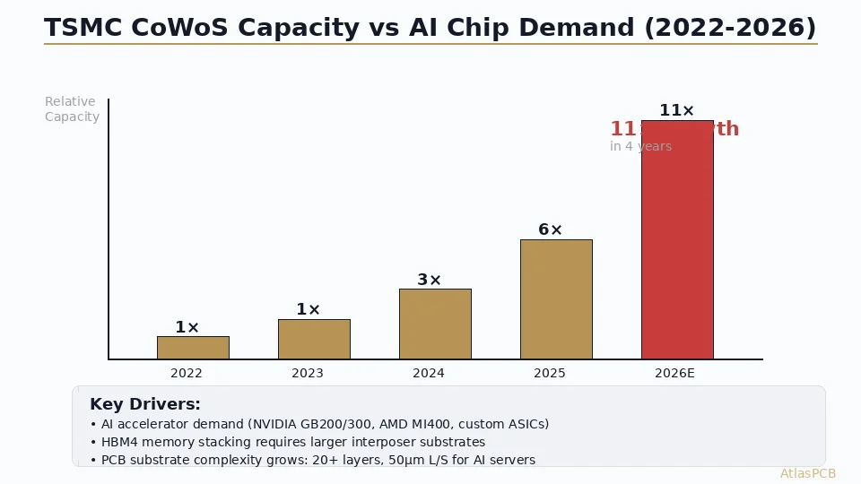
TSMC’s CoWoS (Chip-on-Wafer-on-Substrate) packaging technology is the primary demand driver. Each generation of AI accelerator requires larger, more complex substrates:
| Generation | Interposer Size | Substrate Layers | Die Count |
|---|---|---|---|
| CoWoS-S (H100) | 2,500 mm² | 12-14 layers | 2 (GPU + HBM) |
| CoWoS-L (B200) | 5,000+ mm² | 14-16 layers | 4-6 |
| CoWoS-R (next-gen) | 8,000+ mm² | 16-20 layers | 8+ |
Each doubling of interposer size requires proportional substrate area, more routing layers, and tighter manufacturing tolerances — directly multiplying demand for advanced ABF substrates.
Process Node Transitions: 3nm → 2nm → 1nm
As chip manufacturing moves to smaller process nodes, I/O density increases dramatically. A 2nm chip may have 50-100% more signal connections than its 3nm predecessor, requiring:
- Finer substrate wiring (10μm → 7μm → 5μm L/S)
- More substrate layers (12 → 16 → 20)
- Better dielectric materials (lower Dk/Df for higher data rates)
- Improved via technology (smaller microvias, tighter pitch)
HBM Memory Scaling
High Bandwidth Memory (HBM) stacking is moving from HBM3E (8-12 high) to HBM4 (16+ high). Each HBM stack requires a base die with through-silicon vias (TSVs) connected to the substrate. More HBM stacks per package = more substrate area and more interconnect layers.
Inference AI and Agentic AI
CEO Chen noted that future AI development — specifically inference AI (running trained models) and agentic AI (autonomous AI systems) — could further boost demand for CPUs, ASICs, LPUs (Language Processing Units), and high-end substrates. Unlike training, which is concentrated in a few hyperscale data centers, inference AI deployment is distributed across thousands of edge locations, multiplying total chip volume.
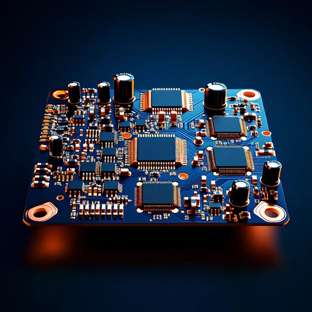
Manufacturing PCBs for AI Infrastructure?
AtlasPCB produces 20-40+ layer boards with low-loss materials, impedance control, and the quality standards required for AI server and networking applications.
Get AI Server PCB Quote →BT Substrates: The Memory and Power IC Backbone
While ABF substrates capture headlines, Kinsus also outlined significant growth in BT (bismaleimide triazine) substrates for:
- HBM memory packaging — base substrates for memory cube stacking
- NAND flash controllers — high-pin-count SSD controller packages
- Power management ICs — substrates for advanced PMICs in AI power delivery
- Optical communication — packages for 800G/1.6T optical transceivers serving AI data center networking
The company noted that existing BT substrate facilities will primarily undergo equipment upgrades rather than new construction, suggesting that growth in BT substrates is more evolutionary than the step-function expansion planned for ABF.
Supply Chain Implications for PCB Manufacturers
Downstream PCB Demand
The substrate boom creates a cascade effect through the PCB supply chain:
AI Server motherboards (20-40 layers): Each AI GPU server requires 1-2 high-layer-count motherboards with:
- Low-loss laminate (Megtron 6/7 or equivalent)
- Heavy copper (2-3oz inner layers) for power delivery
- ±5% impedance tolerance for 56+ Gbps SerDes
- Via-in-pad and backdrilling throughout
Networking switch PCBs (16-24 layers): AI clusters require 400G/800G switches with:
- Ultra-low-loss materials (Df < 0.003)
- Sequential lamination for HDI signal escape
- Precision backdrilling for 112 Gbps PAM4 channels
Power delivery boards (8-16 layers): AI systems consume 2-10 kW per GPU, requiring:
- Heavy copper PCBs (4-6oz)
- High current bus bars
- Thermal management (copper coins, thermal vias)
Material Supply Pressure
AI’s insatiable demand for advanced PCBs is tightening supply of:
- Low-loss laminates — Megtron 6/7 lead times extended to 6-8 weeks
- ABF film — Sole-sourced from Ajinomoto; supply expansion underway but constrained
- Specialty copper foil — Low-profile copper for high-frequency applications seeing allocation
Lead Time Expectations
For hardware companies designing AI infrastructure, expect:
- Standard FR-4 PCBs: 10-15 days (unchanged)
- Low-loss material boards: 15-25 days (material dependent)
- High-layer-count (>20L) with backdrilling: 20-30 days
- ABF substrates: 12-16 weeks (capacity allocated quarterly)
Investment Scale Across the Industry
Kinsus’s expansion is not happening in isolation. Capital expenditure across substrate manufacturers has reached historic levels:
- Kinsus: New factory construction for advanced node substrates
- Ibiden: ¥200B+ investment plan through 2028
- Shinko Electric: Expanding ABF capacity in Japan
- Unimicron: New Taiwan facilities for AI substrates
- Samsung Electro-Mechanics: Korea expansion for FC-BGA
Total industry capex for advanced substrates is estimated at $15-20 billion through 2029 — a scale comparable to semiconductor fab investments.
What This Means for Hardware Engineers
If you’re designing products that use AI accelerators, FPGAs, or high-performance networking chips, the substrate supply chain dynamics affect your planning:
- Lock in packaging early — If your chip uses CoWoS or equivalent, engage substrate suppliers 18-24 months before production
- Design for available substrates — Work with your packaging partner to understand which substrate technologies have capacity
- PCB material planning — Reserve low-loss laminate quantities with your PCB manufacturer for production builds
- Multi-source strategy — Qualify at least two substrate suppliers for production continuity
Further Reading
- AI-Powered EDA Tools Reshaping PCB Design in 2026 — How AI is transforming the design side
- PCB High-Speed Material Dk/Df Comparison — Choosing laminates for AI server boards
- Controlled Impedance PCB Design and Stackup Calculations — Critical for AI infrastructure PCBs
- PCB Copper Plating Thickness Uniformity — Heavy copper for AI power delivery
Source: IC&PCB Union — Kinsus Shareholders Meeting Report, May 2026
Building AI infrastructure? Need high-layer-count, low-loss PCBs? AtlasPCB specializes in 20-40+ layer boards with Megtron 6/7 materials, precision impedance control, and backdrilling for 56 Gbps+ channels. Get a quote for your AI server design →
About AtlasPCB — We specialize in complex PCB manufacturing for HDI, RF, and high-reliability applications. Explore our full PCB manufacturing capabilities, or get an instant online quote . Every order includes free engineering review. Get your quote.
Reviewed by AtlasPCB Engineering Team — IPC-certified manufacturing specialists with 15+ years of production experience in HDI, RF, and high-reliability PCB fabrication. Content based on factory floor data and real customer design reviews.
Frequently Asked Questions
Why is AI driving such long-term substrate demand visibility?
What is an ABF substrate and why does AI need it?
How does this affect regular PCB manufacturers?
- ai-hardware
- pcb-substrate
- abf-substrate
- cowos
- advanced-packaging
- supply-chain
- demand-forecast