· Marcus Lin · Engineering · 6 min read
Copper Roughness and High-Speed Signal Loss
Learn how copper foil surface roughness (Rz) directly increases insertion loss at high frequencies. Compare STD, RTF, HVLP, and ULVP profiles with Huray model predictions for 10–56 Gbps PCB designs.
Quick Answer
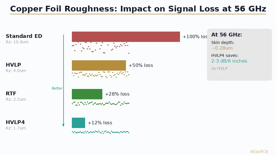
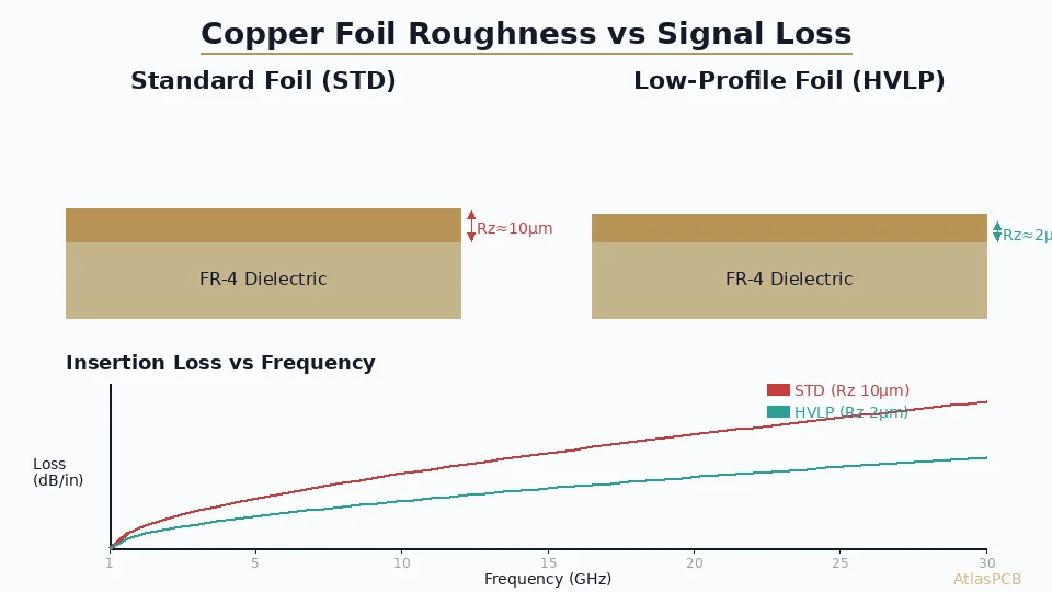
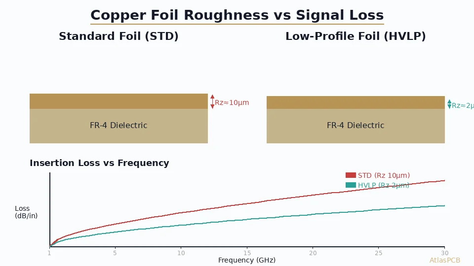
Copper surface roughness increases high-frequency insertion loss because the skin-effect current must travel a longer effective path along the rough conductor surface. At 25 GHz a standard-profile foil (Rz ≈ 10 µm) adds roughly 0.8–1.2 dB/inch more loss than a hyper-low-profile (HVLP) foil (Rz ≈ 2 µm), making foil selection critical for 25G+ SerDes channels.
Why Copper Roughness Matters for High-Speed PCBs
As serial link data rates push beyond 25 Gbps NRZ and into 56–112 Gbps PAM4 territory, every fraction of a decibel in channel loss budget matters. While PCB designers routinely optimize trace width, dielectric thickness, and material Dk/Df, one parameter often receives insufficient attention: copper foil surface roughness.
The copper conductor surface is not optically smooth. Electrodeposited (ED) copper foil has a deliberate “tooth” structure on the matte side that promotes adhesion to prepreg resin during lamination. This roughness forces high-frequency current—concentrated in the skin depth layer—to travel a longer effective path, converting electromagnetic energy into heat.
At 1 GHz the additional loss from roughness is modest (5–15% above smooth-conductor predictions). But roughness loss scales with frequency: at 25 GHz, standard foil can double the conductor loss compared to an ideally smooth surface. For a 12-inch backplane trace, that difference can consume your entire link margin.
How Roughness Increases Conductor Loss
The Skin Effect Foundation
At DC, current distributes uniformly through the conductor cross-section. As frequency increases, current crowds toward the surface. The skin depth δ is:
δ = 1 / √(π·f·µ·σ)
At 10 GHz in copper, δ ≈ 0.66 µm. When surface roughness features (peaks and valleys) are comparable to or larger than the skin depth, the current path becomes tortuous. Instead of flowing in a straight line along the trace length, it must navigate over and around the rough topology.
Roughness-to-Skin-Depth Ratio
The critical parameter is the ratio of RMS roughness to skin depth (Rrms/δ). When this ratio:
- < 0.1: Roughness effect negligible (< 2% additional loss)
- 0.1 to 1.0: Moderate impact (10–50% additional loss)
- > 1.0: Severe impact (50–100%+ additional loss)
For standard ED foil (Rz ≈ 10 µm, Rrms ≈ 3–4 µm), the ratio exceeds 1.0 above ~5 GHz. This is precisely the frequency range where modern high-speed interfaces operate.
The Huray Model
The IPC and IEEE community have adopted the Huray snowball model as the most physically accurate roughness correction factor. Unlike the older Hammerstad model (which saturates at a 2× correction factor), the Huray model represents the rough surface as a collection of spherical protrusions (snowballs) with defined radius and density:
K_rough = 1 + (3/2) · N_sphere · A_sphere · [1/(1 + δ/a)]
Where:
- N_sphere = number of spheres per unit area (tile density)
- A_sphere = surface area of each sphere
- a = sphere radius
- δ = skin depth
This model correctly predicts roughness loss factors of 2.5–3.5× at millimeter-wave frequencies for standard foil, matching measurements from VNA-based insertion loss characterization.
Copper Foil Classification and Selection
Industry-Standard Profiles
The PCB industry classifies copper foil roughness into several grades:
| Profile Grade | Typical Rz (µm) | Rrms (µm) | Common Use |
|---|---|---|---|
| STD (Standard) | 8–12 | 3–5 | General digital, power |
| RTF (Reverse Treated) | 5–8 | 2–3 | Mid-speed digital |
| LP (Low Profile) | 3–5 | 1.2–2 | High-speed 10G–25G |
| VLP/HVLP (Very/Hyper Low Profile) | 1.5–3 | 0.6–1.2 | 25G–56G SerDes |
| ULVP (Ultra-Low Profile) | < 1.5 | < 0.5 | 56G–112G, mmWave |
Manufacturer Specifications
Leading foil manufacturers include:
- Mitsui (MicroThin): HVLP foil with Rz ≤ 2.5 µm
- Fukuda (CF-T9): VLP with controlled nodulation
- Circuit Foil (Lithoglas): ULVP with Rz < 1.5 µm
- Olin (ToughPitch Plus): RTF options for cost-sensitive designs
When specifying laminate materials for high-speed designs, the foil grade is embedded in the laminate product name. For example, Panasonic Megtron 7 is available with both standard and HVLP foil options—always verify which variant your fabricator stocks.
Need Low-Loss PCBs for 25G+ Designs?
AtlasPCB stocks Megtron 6/7 with HVLP foil. We provide impedance simulation and insertion loss correlation before production.
Request a Quote →Quantifying the Loss Difference
Measurement Methodology
To characterize roughness-induced loss, engineers use differential insertion loss testing:
- Fabricate two identical test coupons: one with STD foil, one with HVLP, on the same dielectric
- Measure S21 (insertion loss) using a calibrated VNA from 100 MHz to 50 GHz
- Subtract dielectric loss (known from Dk/Df) to isolate conductor loss
- Compare conductor loss between foil grades
Typical Results (12-inch stripline trace, Dk 3.4)
| Frequency | STD Foil Loss | HVLP Foil Loss | Δ (Savings) |
|---|---|---|---|
| 5 GHz | 3.2 dB | 2.6 dB | 0.6 dB (19%) |
| 10 GHz | 5.1 dB | 3.9 dB | 1.2 dB (24%) |
| 14 GHz (56G PAM4 Nyquist) | 6.5 dB | 4.8 dB | 1.7 dB (26%) |
| 25 GHz | 9.2 dB | 6.5 dB | 2.7 dB (29%) |
| 28 GHz (112G PAM4 Nyquist) | 10.1 dB | 7.0 dB | 3.1 dB (31%) |
At 14 GHz (the Nyquist frequency for 56 Gbps PAM4), switching from STD to HVLP recovers 1.7 dB—often the difference between a passing and failing eye diagram.
PCB Design Implications
Stackup Planning
When specifying a high-speed stackup:
- Signal layers: Use HVLP or ULVP foil on all signal layers carrying 10G+ traffic
- Reference planes: Standard foil is acceptable for ground/power planes since current flows on the plane side facing the signal layer—that surface roughness is the laminate-side profile (typically smoother)
- Cost trade-off: Specify HVLP only where needed. A hybrid approach (HVLP on critical signal layers, STD elsewhere) reduces cost by 15–20% versus all-HVLP construction
Simulation Accuracy
If your SI simulation tool uses a simple Hammerstad roughness model, you may be under-predicting loss for standard foil and over-predicting the benefit of smooth foil. Modern tools (Ansys HFSS, Keysight ADS, Cadence Clarity) support Huray model parameters. Request the sphere radius and hall-sphere tile ratio from your laminate supplier for accurate correlation.
DFM Considerations
Smooth foil creates fabrication challenges:
- Reduced peel strength: Specify oxide-alternative (brown/black oxide) treatment. Minimum peel strength per IPC-6012 Class 3: 6 lb/inch for internal layers
- Delamination risk: Ensure proper plasma desmear and resin-to-foil adhesion testing during first-article qualification
- Pattern plating: HVLP foil may require adjusted imaging parameters due to different surface reflectivity during LDI exposure
Trace Width Adjustment
Lower roughness means slightly lower effective conductor loss, which can allow:
- Narrower traces (saving routing space) while meeting the same loss budget
- Longer traces at the same width while meeting the same loss budget
- Both advantages are modest (5–10%) but meaningful in dense BGA breakout regions
Beyond Roughness: System-Level Loss Budget
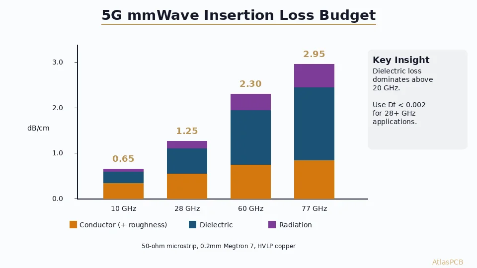
Copper roughness is one component of total channel loss. A complete loss budget includes:
| Loss Mechanism | Typical Contribution (14 GHz, 10-inch stripline) |
|---|---|
| Dielectric loss (Df) | 2.5–4.0 dB |
| Conductor loss (smooth) | 1.8–2.5 dB |
| Roughness adder | 0.8–2.0 dB |
| Via transitions (×2) | 0.5–1.5 dB |
| Connector | 1.0–2.0 dB |
| Total | 6.6–12.0 dB |
The roughness adder represents 10–20% of total channel loss—enough to determine pass/fail for marginal channels.
Practical Guidelines for Engineers
When to Specify HVLP/ULVP
- Always for 25G+ NRZ or 56G+ PAM4 channels
- Recommended for 10G–25G channels longer than 8 inches
- Optional for 10G channels under 6 inches on low-loss dielectrics
- Not needed for sub-5 Gbps interfaces (I²C, SPI, UART, USB 2.0)
Questions for Your Fabricator
- What foil grades are available on your stocked laminates?
- What is the measured Rz and Rrms on your production panels?
- Can you provide Huray model parameters (sphere radius, tile ratio)?
- What peel strength do you achieve with HVLP on [your specified laminate]?
- Do you offer VNA-based insertion loss measurement for qualification?
Cost Impact
HVLP foil typically adds 8–15% to raw laminate cost. For a 16-layer board on Megtron 6:
- STD foil: ~$45/panel
- HVLP on all layers: ~$52/panel (+15%)
- HVLP on signal layers only (6 of 16): ~$48/panel (+7%)
The cost is modest relative to the routing density and performance benefits.
Further Reading
- Signal Integrity PCB Design Guide
- High-Speed Material Dk/Df Comparison
- S-Parameter Characterization of PCB Interconnects
- Controlled Impedance PCB Stackup Design
Ready to optimize your high-speed PCB for minimal signal loss? AtlasPCB provides HVLP and ULVP copper foil options on Megtron 6, Megtron 7, and Tachyon laminates with full impedance simulation and insertion loss verification. Request a quote or explore our capabilities.
About AtlasPCB — We specialize in complex PCB manufacturing for HDI, RF, and high-reliability applications. Explore our impedance-controlled PCB manufacturing, or get an Megtron 6 & 7 low-loss PCB manufacturing . Every order includes free engineering review. Get your quote.
Reviewed by AtlasPCB Engineering Team — IPC-certified manufacturing specialists with 15+ years of production experience in HDI, RF, and high-reliability PCB fabrication. Content based on factory floor data and real customer design reviews.
Frequently Asked Questions
What is copper roughness Rz and how is it measured?
When should I specify HVLP or ULVP copper foil?
Does low-profile copper foil affect PCB adhesion reliability?
- signal integrity
- copper roughness
- HVLP
- high-speed PCB
- insertion loss
- Huray model
- foil profile