· David Okafor · Engineering · 9 min read
HDI PCB Cost Breakdown: Pricing
What does an HDI PCB actually cost? Detailed pricing analysis covering microvia count, sequential lamination cycles, buildup configuration (1+N+1 through 5+N+5), material selection, and practical strategies to reduce HDI cost by 20-40% without sacrificing performance.
Quick Answer
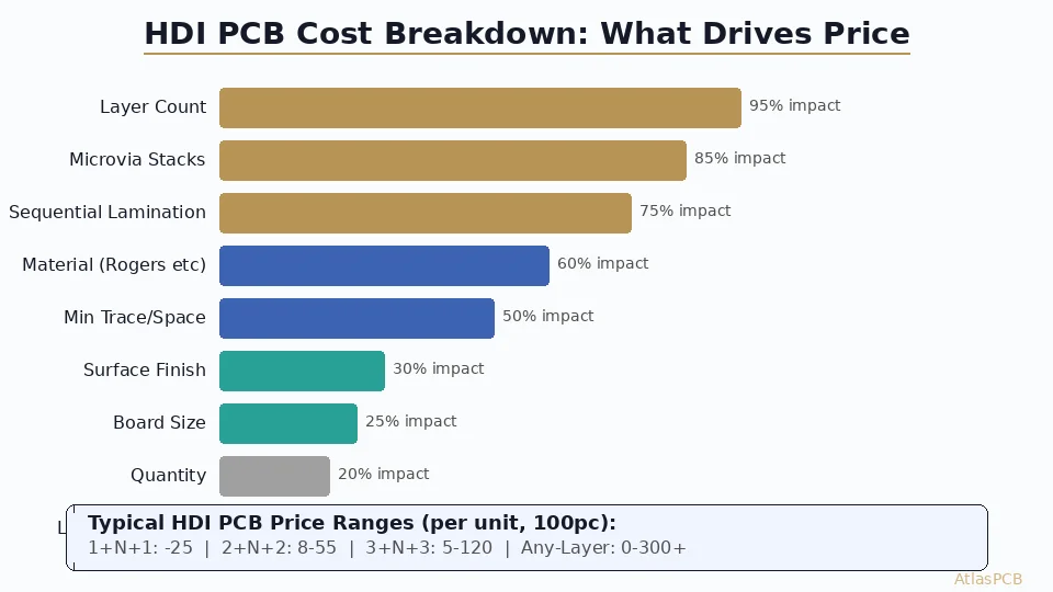
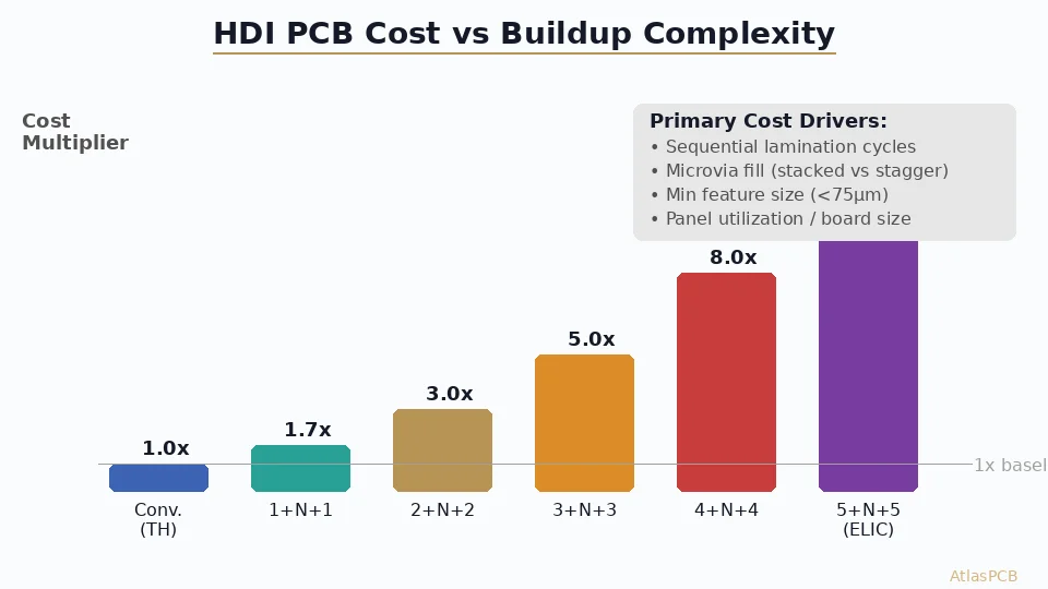
HDI PCB cost ranges from 1.5x (simple 1+N+1) to 8-12x (5+N+5 any-layer) the price of an equivalent conventional through-hole board. The primary cost drivers are sequential lamination cycles (each adds 30-50% to base cost), microvia count and type (stacked vias cost 2-3x more than staggered), and minimum feature size. A 10-layer 2+N+2 HDI in standard FR-4 typically costs $180-400 for 5 prototype pieces, compared to $80-120 for an equivalent 10-layer conventional board.
Cost Overview: HDI vs Conventional PCB
| Configuration | Complexity | Cost vs Conventional | Typical 10-Layer Price (5pc) |
|---|---|---|---|
| Conventional (TH only) | Baseline | 1.0x | $80-120 |
| 1+N+1 (basic HDI) | Low | 1.5-1.8x | $150-200 |
| 2+N+2 (standard HDI) | Medium | 2.5-3.5x | $250-400 |
| 3+N+3 (advanced HDI) | High | 4-6x | $400-700 |
| Any-layer (ELIC) | Very high | 8-12x | $800-1,400 |
These ranges represent standard FR-4 material, 5-piece prototype quantities, 100x100mm board size, with ENIG finish. Your actual pricing varies with board area, material choice, copper weight, and manufacturer capability level. Production quantities (1000+ pieces) reduce the per-unit premium significantly because sequential lamination setup costs are amortized across more boards.
The Five Primary Cost Drivers
1. Sequential Lamination Cycles
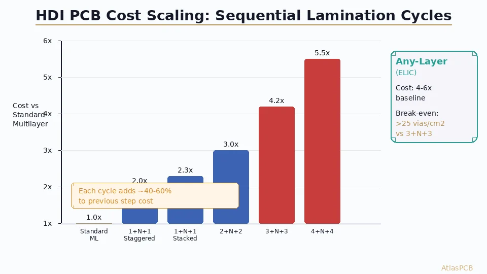
Each ”+” in the HDI buildup notation (1+N+1, 2+N+2) represents a sequential lamination cycle — the board goes back through the entire inner-layer imaging, lamination, drilling sequence for each buildup layer. This is the single largest cost driver because it effectively multiplies the core manufacturing process.
In our production flow, a conventional 10-layer board completes inner layer processing in one pass. A 2+N+2 version of the same board goes through lamination three times: once for the 6-layer core, once to add buildup layers 1 and 10, and once more to add layers 2 and 9. Each cycle adds 1-2 days to manufacturing time and requires precise alignment between existing features and new layers (registration tolerance ±25μm between cycles).
The cost impact is roughly 30-50% per additional cycle because you are essentially paying for the panel to be processed through the factory floor multiple times. A 1+N+1 requires one extra cycle (moderate cost), while 3+N+3 requires three extra cycles (substantial cost). Beyond 3+N+3, the cumulative yield loss from multiple cycles becomes significant — every lamination has a small defect probability that compounds multiplicatively.
HDI SPECIALIST
Get Accurate HDI Pricing — Not Estimates
Upload your Gerber files for a detailed HDI quote with buildup recommendation. We analyze your BGA breakout requirements and suggest the most cost-effective configuration.
Upload for HDI Quote ›
2. Microvia Type and Fill Method
Not all microvias are equal from a cost perspective. The three common configurations, ranked by cost:
Staggered (offset) microvias — cheapest. Each microvia layer is offset from the one below, landing on a solid copper pad. No via filling required because the laser drills into copper, not into a previously drilled hole. Standard electroless + electrolytic plating is sufficient. This is the go-to choice when routing density allows it.
Filled and capped microvias — moderate cost. The microvia is copper-electroplated to fill the hole completely, then the surface is planarized by mechanical grinding. Required when a component pad sits directly over a via (via-in-pad) or when stacking microvias across multiple buildup layers. The filling process adds 45-90 minutes of dedicated plating time per panel plus planarization.
Stacked microvias — highest cost. Multiple buildup layers aligned vertically, each drilled into the filled copper of the layer below. Requires perfect fill quality on every intermediate layer (any void = reliability failure under thermal stress). This demands 100% inspection of fill quality via cross-section sampling, which adds time and reduces yield. Our experience: stacked microvias beyond 3 layers deep require statistical process control monitoring because the failure mode (barrel cracking under thermal cycling) does not appear until reliability testing.
3. Minimum Feature Size
Laser drill diameter directly affects throughput: a 75μm microvia takes roughly the same machine time as a 100μm via, but yield drops noticeably below 75μm due to alignment tolerance consumption. At 50μm (required for some advanced WLCSP and flip-chip packages), yield drops further and many manufacturers add a premium or decline the job entirely.
Similarly, trace/space requirements below 75μm (3/3mil) require modified imaging, etching, and plating processes that reduce throughput. The cost inflection points in our facility:
- 100/100μm (4/4mil): standard process, no premium
- 75/75μm (3/3mil): +10-15% (slower etching, tighter inspection)
- 50/50μm (2/2mil): +40-60% (semi-additive or modified subtractive process)
- Below 50μm: substrate-class processing, 3-5x premium
4. Board Size and Panel Utilization
HDI panels run through expensive sequential lamination equipment that operates on fixed panel sizes (typically 18x24” production panels). Your board’s outline determines how many pieces fit per panel, and you pay per panel-pass through the process. A 30x30mm module board fits 30+ pieces per panel, making each sequential lamination cycle cheap per-unit. A 200x150mm main board fits only 4 pieces per panel, making each cycle expensive per-unit.
Based on panels we have run across hundreds of HDI orders, the per-unit cost sweet spot is board area between 20x20mm and 80x80mm. Below 20mm, routing/handling overhead dominates. Above 100mm per side, you are consuming significant panel real estate and yield risk increases with board area.
COST OPTIMIZATION
We Recommend the Cheapest HDI Build That Works
Our engineers analyze your design and suggest optimizations: staggered vs stacked, buildup reduction, via diameter increases — saving 20-40% without compromising functionality.
Get Optimized Quote ›5. Material Selection Impact on HDI Cost
Standard mid-Tg FR-4 (Tg 150-170) is the default HDI material and adds zero material premium. However, many HDI designs require high-Tg (Tg 170+) material for reliability under multiple reflow cycles — the additional lamination cycles in HDI manufacturing subject the board to more thermal stress during production, and high-Tg material resists that stress better.
Material premium for HDI boards:
- Standard FR-4 (Tg 150): baseline
- High-Tg FR-4 (Tg 170): +5-10%
- Low-loss material (Megtron 6, Panasonic R-5775): +30-50%
- Rogers hybrid (Rogers RF + FR-4 digital with HDI): +80-150%
- Halogen-free: +5-8%
For designs combining HDI with specialty materials (common in 5G infrastructure and data center networking), the cost compounds — you are paying both the HDI process premium and the material premium simultaneously.
Budget Optimization: Practical Strategies
Strategy 1: Reduce Buildup When Possible
Challenge your assumption about HDI necessity. We regularly review designs where the engineer specified 2+N+2 but could achieve the same breakout with 1+N+1 by using slightly wider traces on the core layers or shifting a few signals to different layers. The cost difference between 1+N+1 and 2+N+2 for a 10-layer board is typically $100-200 at prototype quantities (5 pieces).
Strategy 2: Asymmetric Buildups
If your high-density components concentrate on one side of the board (common for SoC-centric designs), specify an asymmetric buildup: 2+N+1 instead of 2+N+2. The top side gets two buildup layers for BGA breakout while the bottom side uses a single buildup or conventional through-holes only. Cost savings: 15-25% versus the symmetric equivalent.
Strategy 3: Increase Microvia Diameter
If your design routes at 75μm trace/space, you likely have room to increase microvia diameter from the minimum 75μm to 100μm or even 125μm. Larger vias drill faster (higher throughput), yield better (less sensitive to alignment), and plate more uniformly. Moving from 75μm to 100μm microvias typically saves 10-15% on overall board cost due to improved yield alone.
Strategy 4: Production Volume Leverage
HDI economics improve dramatically at volume because sequential lamination setup costs are fixed per lot, not per board. The crossover point where HDI becomes economically comparable to adding conventional layers (just making the board bigger or using more layers to avoid HDI) is typically around 200-500 pieces for 1+N+1 builds.
At 5,000+ pieces, a 1+N+1 HDI design that consolidates a 12-layer conventional board into an 8-layer HDI can actually be cheaper per unit because you are paying for fewer total layers of processing — the HDI cycle cost is offset by eliminating 4 conventional layers.
HDI PCB MANUFACTURER
From 1+N+1 to 5+N+5 — In-House Laser Drill Capacity
We operate our own CO2 and UV laser drill systems — no outsourcing markup. Combined with in-house sequential lamination, we deliver competitive HDI pricing with fast turnaround.
View HDI Capabilities ›When HDI Is Actually Worth the Premium
The decision to use HDI should be driven by either routing necessity (cannot break out BGAs without microvias) or total system cost optimization (HDI enables a smaller board that reduces enclosure cost, improves thermal performance, or reduces connector count).
The engineering case for HDI is strongest when: your BGA pitch is 0.5mm or below with high pin count (200+), your board area is constrained by the product enclosure, you need signal integrity performance that shorter via stubs enable (25+ Gbps signaling), or you can consolidate layer count (12L conventional to 8L HDI) to reduce total manufacturing cost at production volumes.
The case against HDI: if dog-bone breakout with conventional vias achieves your routing, if your board has physical space for additional conventional layers, or if your production volume is below 50 pieces and redesign for conventional routing would take less time than the HDI cost premium justifies.
ATLASPCB
Get Your HDI PCB Quote in 24 Hours
Upload Gerber files for instant HDI pricing with buildup optimization recommendations. We process 1+N+1 through 5+N+5, stacked and staggered microvias, via-in-pad with planarization.
Get HDI Quote ›
Reviewed by AtlasPCB Engineering Team — 15+ years in advanced PCB fabrication for RF, HDI, and rigid-flex applications.
Related Reading:
About AtlasPCB — We specialize in complex PCB manufacturing for HDI, RF, and high-reliability applications. Explore our HDI PCB manufacturing capabilities, or get an instant online PCB quote . Every order includes free engineering review. Get your quote.
Reviewed by AtlasPCB Engineering Team — IPC-certified manufacturing specialists with 15+ years of production experience in HDI, RF, and high-reliability PCB fabrication. Content based on factory floor data and real customer design reviews.
Frequently Asked Questions
How much more expensive is HDI PCB compared to standard PCB?
What is the cheapest HDI PCB configuration?
Why do stacked microvias cost more than staggered?
How can I reduce HDI PCB cost without changing the design?
At what BGA pitch do I actually need HDI?
- HDI PCB
- PCB cost
- PCB pricing
- microvia
- sequential lamination
- HDI PCB manufacturer