· David Okafor · Engineering · 7 min read
PCB Prototype Cost Breakdown
Transparent breakdown of PCB prototype pricing: setup fees, material costs, drilling, plating, and testing. Learn what drives cost at low volumes and how to optimize your prototype order for maximum value.
Quick Answer
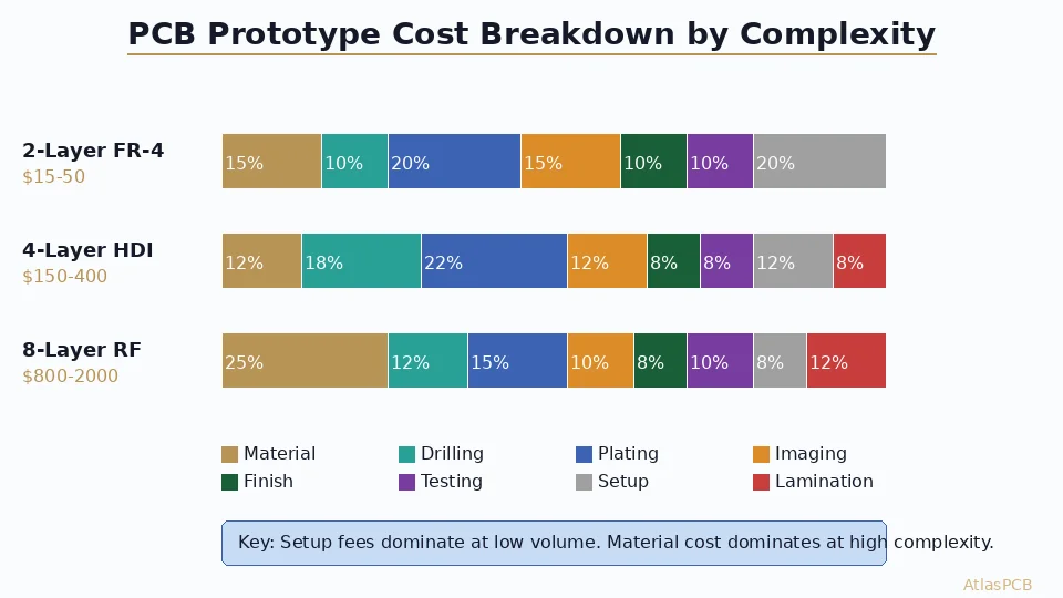
A 2-layer FR-4 PCB prototype (100x100mm, 5 pieces) costs $15-50 with standard 5-day lead time. A 4-layer board of the same size runs $80-200. Costs jump to $500-2000+ for HDI or RF prototypes. The biggest cost drivers at prototype volumes are setup/tooling fees (30-40% of total) and minimum order charges, not material. To save 30-50%: consolidate designs into one panel, use standard materials, avoid blind/buried vias unless necessary, and choose 5-7 day lead time over rush.
Prototype Price Ranges at a Glance
| Board Type | 5 pcs / 100x100mm | Lead Time | Key Cost Driver |
|---|---|---|---|
| 2-layer FR-4 | $15-50 | 3-5 days | Setup fee |
| 4-layer FR-4 | $80-200 | 5-7 days | Lamination + setup |
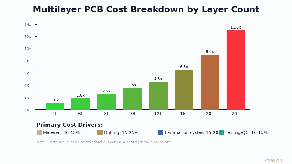
| 6-layer FR-4 | $150-350 | 7-10 days | Lamination cycles |
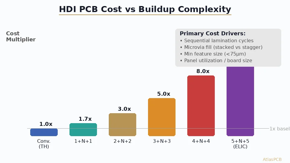
| 4-layer HDI (1+2+1) | $200-500 | 8-12 days | Laser drill + sequential lam |
| 6-layer HDI (2+2+2) | $400-900 | 10-15 days | Multiple sequential lam |
| RF (Rogers/PTFE, 2L) | $200-600 | 7-10 days | Material cost |
| Rigid-flex (4L rigid + 2L flex) | $500-1500 | 12-18 days | Flex material + assembly |
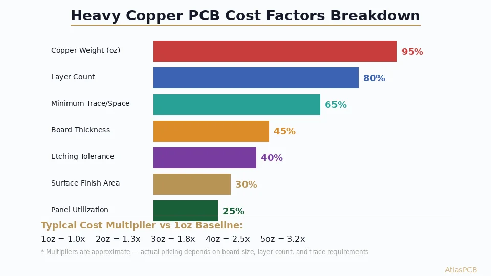
These ranges assume standard specs (1oz copper, ENIG, no special testing). Add 20-50% for controlled impedance, heavy copper, or non-standard drill requirements.
Where Your Money Actually Goes
At Prototype Volumes (5-10 pieces)
The cost structure at prototype quantities is fundamentally different from production:
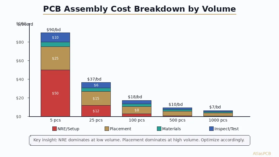
Fixed costs (independent of quantity):
- CAM engineering review: $15-30
- Photo tool/imaging setup: $10-20 per layer pair
- Drill file programming: $5-10
- Impedance coupon (if required): $20-40
- Electrical test fixture: $10-30
Semi-variable costs:
- Material (panel allocation): $5-20 per board
- Drilling: $3-8 per board
- Plating (chemistry and time): $5-15 per board
- Etching and imaging: $3-8 per board
- Surface finish: $2-10 per board
- Final inspection: $3-5 per board
At 5 pieces, fixed costs represent 40-60% of your total order price. At 50 pieces, they drop to 10-15%.
This is the fundamental insight: Ordering 10 boards instead of 5 typically costs only 30-40% more — the marginal cost per additional board is low because fixed costs are already covered.
INSTANT PRICING
See Exact Prototype Cost in 30 Seconds
Upload Gerber files for instant automated pricing. No account required. See cost breakdown by layer count, finish, and lead time.
Get Instant Quote ›
The 7 Biggest Cost Multipliers (and How to Avoid Them)
1. Layer Count: +30-40% Per Layer Pair
Every additional layer pair (two copper layers + one prepreg sheet) adds:
- Material cost (copper foil + prepreg)
- An additional imaging and etching cycle
- Alignment registration requirements
- Lamination press time
Optimization: Challenge whether you need 6 layers. Many 6-layer designs can fit on 4 layers by:
- Increasing board area by 15-20% for routing space
- Using 0.3mm vias instead of 0.2mm (eases routing density)
- Combining power and ground into split planes
2. Via Technology: +30-80% for Blind/Buried
| Via Type | Cost Impact | When Required |
|---|---|---|
| Through-hole (standard) | Baseline | Default choice |
| Blind via (L1-L2) | +30-50% | BGA fanout on HDI |
| Buried via (L2-L3) | +40-60% | Inner-layer routing |
| Stacked microvia | +60-80% | High-density BGA (>1000 pins) |
| Via-in-pad (VIPPO) | +20-30% | Fine-pitch BGA, thermal pads |
Optimization: Before using blind/buried vias, try:
- Dog-bone fanout with through-hole vias (works for 0.8mm+ pitch BGA)
- Back-drilling instead of blind vias for high-speed signals (cheaper and better signal integrity)
- Through-hole vias with larger board area for routing escape
3. Material Selection: 2-10x Premium for Specialty Laminates
| Material | Relative Cost | Typical Application |
|---|---|---|
| Standard FR-4 (Tg 135C) | 1x | General electronics |
| High-Tg FR-4 (Tg 170C) | 1.2-1.5x | Lead-free assembly, automotive |
| Low-Dk FR-4 (Megtron 6) | 2-3x | >10 Gbps signals |
| Rogers RO4350B | 3-5x | RF up to 20 GHz |
| PTFE (Rogers RT/duroid) | 5-8x | mmWave, 28+ GHz |
| Polyimide (flex) | 3-5x | Flex/rigid-flex |
Optimization: Use specialty material only on layers that need it. Mixed stackups (Rogers on outer + FR-4 core) save 30-50% vs all-Rogers. See our Rogers vs PTFE selection guide for RF applications.
4. Surface Finish: $0 to $50+ Difference
| Finish | Prototype Cost (5 pcs, 100mm2) | Best For |
|---|---|---|
| HASL (leaded) | Cheapest ($0 premium) | Non-fine-pitch, not RoHS |
| HASL (lead-free) | +$3-5 | Budget, standard SMT |
| OSP | +$0-2 | Immediate assembly |
| ENIG | +$8-15 | Fine-pitch, storage |
| Immersion Silver | +$5-10 | Flat, cost-conscious |
| Hard Gold (edge connectors) | +$20-50 | Card-edge, high-wear |
Optimization: HASL is cheapest but not flat enough for fine-pitch. ENIG is the “safe default” for prototypes since boards may sit before assembly. Avoid specifying Hard Gold unless you have card-edge connectors.
5. Board Size and Panelization
Most fabricators run prototype orders on shared “pool panels” (multiple customers’ boards on one production panel). Your cost is proportional to the panel area you consume:
- Under 50x50mm: Extremely cost-efficient (many copies fit one slot)
- 50-100mm per side: Standard sweet spot
- 100-200mm: May need 2 panel slots
- Over 200mm: Likely needs dedicated panel → significant cost jump
Optimization: If your board is 110x110mm, check whether reducing to 100x100mm drops it into a smaller panel slot. That 10% area reduction could save 30-40% on prototype cost.
6. Minimum Drill Size: Smaller = More Expensive
| Drill Size | Cost Impact | Notes |
|---|---|---|
| 0.3mm+ (mechanical) | Standard | No premium |
| 0.2mm (mechanical) | +10-15% | Requires slower feed rate |
| 0.15mm (mechanical min) | +20-30% | High drill breakage rate |
| 0.1mm (laser) | +40-60% | Requires laser drill equipment |
| 0.075mm (laser) | +50-80% | HDI microvia |
Optimization: Use 0.3mm vias as default. Only go smaller when routing density absolutely requires it.
7. Lead Time: Rush Fees Are Real
Standard lead time is 5-7 days for 4-layer boards. Faster costs more:
| Lead Time | Premium | Why |
|---|---|---|
| 5-7 day | Standard | Normal production flow |
| 3 day | +40-60% | Priority scheduling |
| 48-hour | +80-150% | Overtime + expedited material |
| 24-hour (2L only) | +100-200% | Dedicated line time |
Optimization: Plan ahead. The difference between 3-day and 7-day delivery on a 4-layer prototype can be $100-200. If you’re iterating, order boards at standard lead time while you continue firmware/software development.
COST COMPARISON
Compare Price Across Lead Times Instantly
Our quote system shows pricing for 3-day, 5-day, 7-day, and standard options side by side. Pick the cost-schedule tradeoff that works for your sprint.
Compare Lead Times ›5 Strategies to Cut Prototype Cost by 30-50%
Strategy 1: Consolidate Multiple Designs per Order
If you have 3 different board designs for the same project (main board + daughter card + sensor board), submit them as one order with panelized delivery. You pay one setup fee instead of three, and shared panel space reduces per-board material cost.
Savings: 25-40% vs three separate orders.
Strategy 2: Order 10 Instead of 5
Counter-intuitive but mathematically sound. The fixed-cost dominance means:
- 5 boards at $80 = $16/board
- 10 boards at $100 = $10/board
The extra 5 boards serve as assembly spares, testing sacrificials, or backup for rework damage.
Strategy 3: Use Standard Everything
The lowest-cost prototype uses:
- Standard FR-4, 1.6mm, 1oz copper
- 0.3mm minimum drill (no microvias)
- Through-hole vias only
- HASL or ENIG surface finish
- Green solder mask (fastest processing — dedicated lines)
- No impedance control (unless actually required for your signals)
Each “special” specification triggers additional processing steps, setup time, and sometimes material procurement delays.
Strategy 4: Design for Standard Panel Utilization
Work with your fabricator’s standard panel sizes. AtlasPCB uses 18”x24” (457x610mm) production panels. If your board dimensions allow efficient tiling:
- 50x50mm: 80+ boards per panel (very efficient)
- 100x100mm: 20+ boards per panel (good)
- 160x100mm: 12+ boards per panel (acceptable)
- 200x250mm: 4 boards per panel (expensive per board)
Strategy 5: Skip Unnecessary Testing at Prototype Stage
Full electrical testing (flying probe) adds $10-30 per prototype order. For a 5-piece prototype run where you’ll be debugging anyway:
- Request visual inspection only (saves $10-20)
- Add electrical testing only for production orders where yield data matters
However: if your board has fine-pitch BGAs or blind vias, flying probe testing is worth the cost to catch opens/shorts before expensive assembly.
PROTOTYPE SPECIALISTS
Prototype-Optimized Pricing from 2 to 30 Layers
AtlasPCB runs dedicated prototype lines with pooled panels to minimize per-board cost. Upload your design for transparent cost breakdown.
Upload Design ›Real Example: Same Design, 3 Different Prices
Consider a 4-layer board, 80x60mm, with a BGA processor and DDR4 memory:
| Configuration | Price (10 pcs) | Notes |
|---|---|---|
| Standard | $120 | FR-4, ENIG, through-hole vias, 7-day |
| Over-specified | $380 | High-Tg, impedance control, blind vias, 3-day |
| Optimized | $95 | FR-4, HASL, through-hole, 7-day, no impedance coupon |
The “over-specified” board has blind vias that aren’t necessary (BGA pitch is 0.8mm — fanout works with through-holes), impedance control that could be achieved with trace width adjustment alone, and rush delivery that wasn’t needed.
The “optimized” version uses HASL (acceptable since the BGA pitch is 0.8mm) and skips the impedance test coupon (still manufactures to controlled impedance but without the formal verification — acceptable for a prototype).
Savings: 75% reduction by questioning every specification.
ATLASPCB
Get Your Prototype Quote in Under 60 Seconds
Instant pricing with full cost breakdown. See exactly what drives your board cost and where to save.
Get Instant Quote ›
Related Reading:
About AtlasPCB — We specialize in complex PCB manufacturing for HDI, RF, and high-reliability applications. Explore our PCB prototype manufacturing from 1 piece, quick-turn PCB manufacturing from 24 hours, or get an instant online PCB quote . Every order includes free engineering review. Get your quote.
Reviewed by AtlasPCB Engineering Team — IPC-certified manufacturing specialists with 15+ years of production experience in HDI, RF, and high-reliability PCB fabrication. Content based on factory floor data and real customer design reviews.
Frequently Asked Questions
Why are PCB prototypes so expensive per board compared to production?
What is the cheapest way to prototype a 4-layer PCB?
Does board size significantly affect prototype cost?
How much does rush delivery add to PCB prototype cost?
- PCB cost
- prototype pricing
- PCB manufacturing cost
- cost optimization
- quick-turn PCB