· David Okafor · Engineering · 4 min read
PCB Cost Optimization
Reduce PCB costs without sacrificing quality — practical tips for layer count reduction, panel optimization, material selection, design simplification, and volume pricing strategies.

Quick Answer
PCB cost is driven by layer count, board size, material type, via technology, surface finish, and order quantity. Key optimization strategies include panelization, standard materials, avoiding unnecessary HDI/blind vias, and consolidating orders for volume pricing.
PCB cost can represent 5-30% of a product’s total BOM, depending on complexity. Small design changes can yield significant savings at volume. Here are 15 practical strategies to reduce PCB cost.
Fabrication Cost Drivers
1. Reduce Layer Count
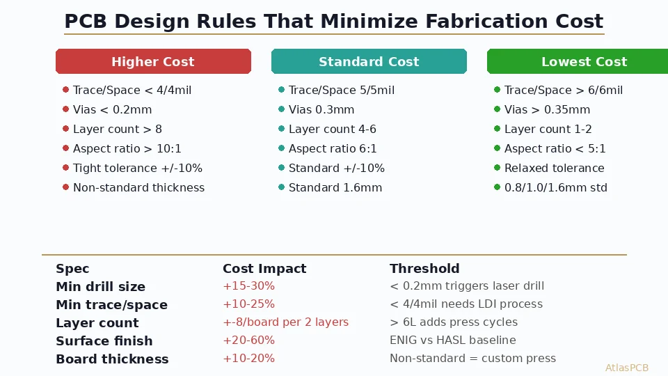
The single biggest cost factor. Each additional layer pair adds 30-40% to board cost.
Action: Challenge whether you truly need 6 layers. Many designs can fit on 4 layers with creative routing. Consider increasing board size slightly to enable fewer layers.
| Layers | Relative Cost |
|---|---|
| 2 | 1.0x |
| 4 | 2.0-2.5x |
| 6 | 3.0-3.5x |
| 8 | 4.0-5.0x |
2. Use Standard Board Thickness
1.6mm is the industry standard and cheapest option. Non-standard thicknesses (0.8mm, 1.0mm, 2.0mm) add 5-15% due to special material requirements.
3. Use Standard Copper Weight
1oz copper is the default. 2oz adds 15-25%. Only use heavy copper where actually needed — use copper pours instead of wide traces for current-carrying paths.
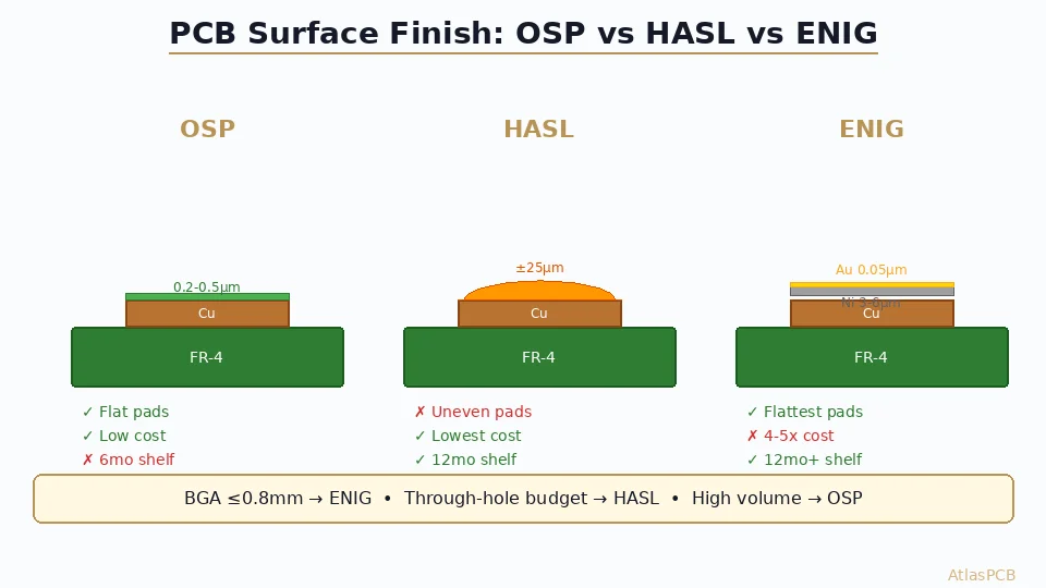
4. Choose Standard Surface Finish
- HASL (cheapest) → OSP → Immersion Tin → Immersion Silver → ENIG (most expensive)
- If you don’t need fine-pitch BGA, HASL or OSP may suffice
5. Optimize Panel Utilization
Poor panel utilization wastes material. Work with your manufacturer to maximize the number of boards per panel.
Tips:
- Standard panel sizes vary by manufacturer — ask for their optimal sizes
- Rotating boards 90° may improve fit
- Combine multiple designs on one panel (if quantities match)
- Target >80% utilization
6. Relax Design Rules
Tighter design rules (3/3 mil trace/space) require more precise equipment and lower yields than standard rules (5/5 mil). Use the loosest rules your design allows.
| Feature | Standard (Cheaper) | Advanced (Pricier) |
|---|---|---|
| Trace/space | 5/5 mil | 3/3 mil |
| Drill size | 0.3mm | 0.15mm |
| Annular ring | 5 mil | 3 mil |
7. Minimize Drill Count and Sizes
Each unique drill size requires a tool change. More holes = longer drilling time = higher cost.
- Standardize via sizes (use one or two via sizes for the entire board)
- Avoid unnecessary mounting holes
- Combine test point vias with routing vias where possible
8. Avoid Blind and Buried Vias
Through-hole vias are 30-50% cheaper than blind/buried vias. Only use advanced via types when routing density absolutely requires it.
9. Standard Solder Mask Color
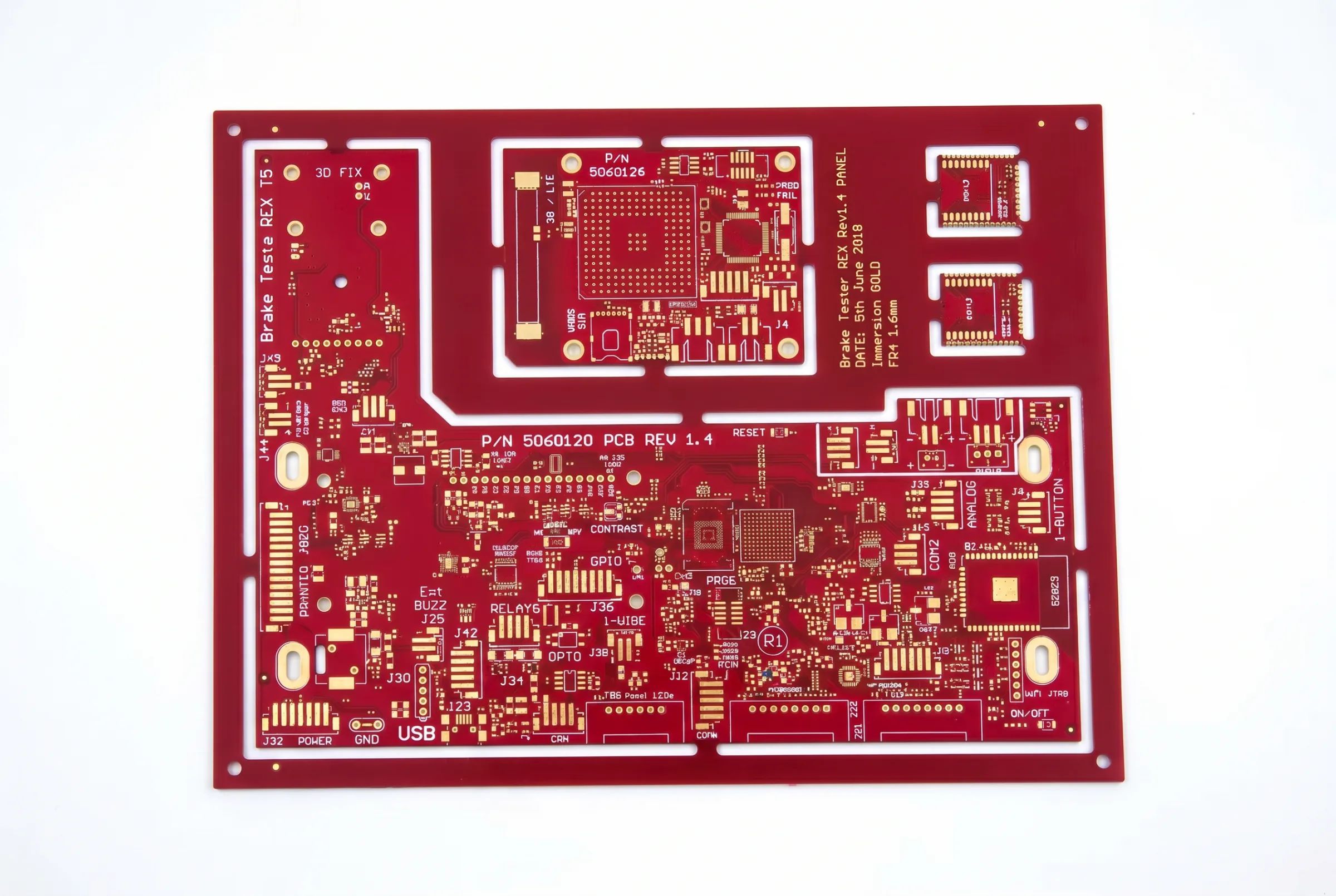
Green is cheapest. Other colors (black, white, red, blue) add 5-10%.
10. Standard Silkscreen
White silkscreen on green mask is cheapest. Yellow or black silkscreen, or silkscreen on both sides, adds cost.
Assembly Cost Drivers
11. Reduce Component Count
Fewer components = less assembly time = lower cost. Look for integrated solutions (e.g., SoC vs MCU + peripherals).
12. Single-Side Assembly
Populating both sides of the board requires two reflow passes, doubling assembly time. Design for single-side placement when possible.
13. Avoid Mixed Technology
Pure SMT assembly is cheaper than mixed SMT + through-hole, which requires additional wave or selective soldering steps.
14. Standard Component Packages
Use common packages (0402, 0603, 0805 for passives; SOIC, QFP, QFN for ICs). Unusual packages may require special feeder setup.
15. Design for Automated Assembly
- Adequate spacing between components (>0.5mm)
- Fiducial marks for pick-and-place alignment
- No components in keep-out zones
- Consistent component orientation
Volume Pricing Strategy
| Quantity | Typical Discount |
|---|---|
| 1-10 | Base price (prototype pricing) |
| 50-100 | 20-40% off base |
| 500-1,000 | 40-60% off base |
| 5,000-10,000 | 60-75% off base |
| 50,000+ | 75-85% off base |
Tip: Order in quantities that match price break points. Ordering 95 boards vs 100 may cost more per unit if 100 is a price break.
Quick Cost Estimation Formula
PCB cost ≈ Base area cost x Layer multiplier x Feature multiplier
Where:
- Base area cost: $0.01-0.05/cm2 (depending on volume)
- Layer multiplier: 1x (2L), 2.2x (4L), 3.2x (6L), 4.5x (8L)
- Feature multiplier: 1x (standard), 1.3x (fine features), 1.5x (HDI)
Conclusion
The biggest cost savings come from reducing layers, optimizing panel utilization, and using standard materials and processes. Many of these decisions must be made during the design phase — changing them later is expensive. Share your cost targets with your PCB manufacturer early; they can often suggest design modifications that save money without affecting performance.
Further Reading
[HDI PCB Design Guide: Stackup Rules, Via Structures & DFM Checklist]/blog/hdi-pcb-design-guide/)
[ENEPIG vs ENIG: Which PCB Surface Finish for Your Design?]/blog/enepig-vs-enig/)
[PCB Surface Finish Guide: HASL, ENIG, OSP and More Compared]/blog/pcb-surface-finish-guide/)
[PCB Solder Mask: Types, Colors, and Functions Explained]/blog/pcb-solder-mask-guide/)
[Heavy Copper PCB: Design Rules, Manufacturing Limits, and Thermal Management]/blog/heavy-copper-pcb/)
[PCB Manufacturer with Engineering Review: Why Human DFM Audit Matters]/blog/pcb-manufacturer-engineering-review/)
[PCB Thermal Management: Heat Dissipation Techniques for Reliable Electronics]/blog/pcb-thermal-management/)
About AtlasPCB — We specialize in complex PCB manufacturing for HDI, RF, and high-reliability applications. Explore our free engineering DFM review, or get an full PCB manufacturing capabilities . Every order includes free engineering review. Get your quote.
Reviewed by AtlasPCB Engineering Team — IPC-certified manufacturing specialists with 15+ years of production experience in HDI, RF, and high-reliability PCB fabrication. Content based on factory floor data and real customer design reviews.
Frequently Asked Questions
What factors affect PCB manufacturing cost?
How much does a PCB prototype cost?
How can I reduce PCB cost without sacrificing quality?
- cost optimization
- pcb manufacturing
- DFM
- production