· David Okafor · Engineering · 7 min read
How to Specify Annular Ring Requirements
Complete engineering guide for specifying annular ring width in PCB designs. Covers IPC-6012 Class 2 vs Class 3, minimum values for HDI microvias, and common DFM errors that cause pad breakout.
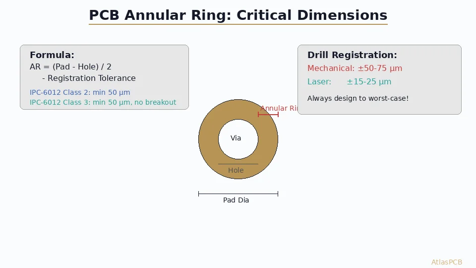
Quick Answer
For IPC-6012 Class 2 (standard electronics), minimum annular ring is 50 µm (2 mil) after drilling and plating. For Class 3 (high reliability), minimum is 50 µm with zero breakout allowed on any layer. For HDI microvias (laser-drilled ≤150 µm), minimum annular ring is typically 75 µm (3 mil) on capture pad and 50 µm on target pad. Always specify your annular ring as the MINIMUM REMAINING after drill tolerance—not just pad diameter minus drill size. Most DFM failures come from designers forgetting to account for ±75 µm drill registration tolerance on mechanical drills.
Why Annular Ring Specs Kill PCBs in Fabrication
The annular ring—the copper remaining between the edge of a drilled hole and the edge of its pad—is the #1 source of DFM rejections we see at AtlasPCB. Engineers specify pad sizes and drill sizes independently in their EDA tools without calculating the resulting annular ring under worst-case registration conditions. The result: designs that look fine on screen but fail in manufacturing.
This guide walks you through proper annular ring specification, from basic calculations to advanced HDI scenarios, with the exact numbers your fabricator needs.
The Fundamentals
What Your Fabricator Actually Sees
When you send Gerber files, your fabricator sees:
- Pad diameter (from copper layer Gerbers)
- Drill diameter (from the NC drill file)
- The math between them determines annular ring
The problem: your drill doesn’t land perfectly centered on the pad. Every mechanical drill has registration tolerance—typically +/-50 to +/-75 µm—meaning the hole can shift from nominal position. Your annular ring must survive this shift.
The Critical Formula
Minimum Annular Ring = (Pad Diameter - Finished Hole Diameter) / 2 - Registration ToleranceExample—Standard Through-Hole Via:
- Pad diameter: 0.7 mm (28 mil)
- Finished hole: 0.35 mm (14 mil)
- Drill registration: +/-0.075 mm (+/-3 mil)
- Annular ring: (0.7 - 0.35) / 2 - 0.075 = 0.100 mm (4 mil)
This provides comfortable margin above the IPC-6012 Class 2 minimum of 0.050 mm.
FREE DFM REVIEW
We Check Annular Ring Compliance on Every Order
Upload your Gerbers and our engineers verify annular ring across all layers — flagging breakout risk before fabrication starts.
Upload Gerbers ›
IPC-6012 Requirements by Class
| Parameter | Class 1 (General) | Class 2 (Dedicated) | Class 3 (High Reliability) |
|---|---|---|---|
| Minimum annular ring (external) | 50 µm (breakout OK) | 50 µm (breakout OK on up to 20% of PTHs) | 50 µm (zero breakout) |
| Minimum annular ring (internal) | N/A | 0 µm (tangent allowed) | 50 µm (zero breakout) |
| Breakout allowance | 90 deg per side | 90 deg per side, max 20% of vias | Not allowed |
| Applicable products | Consumer, toys | Commercial electronics, telecom | Military, aerospace, medical |
What “Breakout” Means
Breakout occurs when the drill hole extends beyond the pad copper boundary on one or more layers. For Class 2, limited breakout is acceptable—the via barrel still connects through copper plating inside the hole. For Class 3, ANY breakout on ANY layer is a reject condition. This is why aerospace and medical designs need larger pads relative to holes.
Recommended Design Rules by Via Type
Standard Through-Hole Vias (Mechanical Drill)
| Via Type | Finished Hole | Minimum Pad | Annular Ring (worst-case) | Target Application |
|---|---|---|---|---|
| Signal via | 0.25 mm | 0.55 mm | 75 µm | Dense routing (8+ layers) |
| Signal via | 0.30 mm | 0.60 mm | 75 µm | Standard routing |
| Power via | 0.35 mm | 0.70 mm | 100 µm | Power distribution |
| Component TH | 0.80 mm | 1.30 mm | 175 µm | Through-hole connectors |
| Mounting hole | 3.20 mm | 4.00 mm | 325 µm | Mechanical fasteners |
HDI Microvias (Laser Drill)
| Via Type | Finished Hole | Capture Pad | Target Pad | AR (capture) | AR (target) |
|---|---|---|---|---|---|
| Standard microvia | 100 µm | 275 µm | 250 µm | 75 µm | 62 µm |
| Fine-pitch microvia | 75 µm | 225 µm | 200 µm | 62 µm | 50 µm |
| Ultra-fine microvia | 50 µm | 175 µm | 150 µm | 50 µm | 37 µm |
Laser drills have +/-15–25 µm registration (vs +/-50–75 µm for mechanical), enabling smaller pads. However, the plating process requires adequate copper area for reliable via fill.
Common DFM Errors We Catch
After reviewing thousands of designs, here are the annular ring errors we see most frequently:
Error 1: Ignoring Registration Tolerance
The mistake: Designer sets pad = 0.5 mm, drill = 0.3 mm, calculates (0.5-0.3)/2 = 0.1 mm annular ring. “That’s well above 50 µm minimum!”
The reality: After +/-75 µm drill registration, worst-case annular ring = 0.1 - 0.075 = 0.025 mm—below IPC minimum.
The fix: Always calculate worst-case. Add your fab’s stated registration tolerance to the minimum required annular ring.
Error 2: Different Drill Sizes Share One Pad Size
The mistake: Using the same 0.5 mm pad for both 0.2 mm vias (fine) and 0.35 mm vias (marginal at 0.5 mm pad with tolerances).
The fix: Define pad size per drill size in your design rules. Most EDA tools support this with via definitions or padstack editors.
DFM EXPERTISE
Avoid Costly Respins — Get It Right the First Time
Our engineering review catches pad/drill mismatches, registration issues, and IPC compliance problems before production.
Start DFM Review ›Error 3: Forgetting Inner Layer Registration
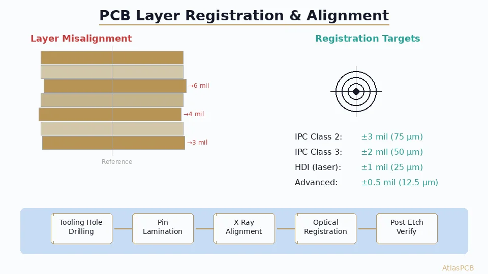
The mistake: Outer layer pads are fine, but inner layer registration is different (worse) due to lamination shift. On a 20-layer board, inner layers can shift +/-100 µm relative to the drill.
The fix: For high-layer-count boards (>12 layers), increase inner layer pads by 50–100 µm relative to outer layer pads, or use non-functional pads (NFPs) on routing layers and full pads on reference layers.
Error 4: BGA Fanout Without Checking AR
The mistake: Using 0.275 mm pads to achieve 0.5 mm BGA dog-bone fanout without verifying the resulting annular ring with a 0.15 mm via hole.
The fix: AR = (0.275 - 0.15) / 2 - tolerance. With +/-50 µm mechanical drill: AR = 0.0625 - 0.05 = 0.0125 mm. That’s below minimum. Either use laser microvias (better registration) or increase the pad to 0.325 mm and accept one less routing channel.
How to Specify Annular Ring in Your Fab Drawing
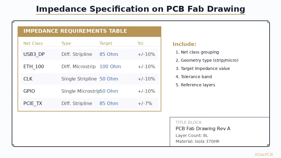
Your fabrication drawing should explicitly state:
ANNULAR RING REQUIREMENTS:
- External layers: Minimum 75 µm (3 mil) after plating
- Internal layers: Minimum 50 µm (2 mil) after plating
- Microvias: Minimum 62 µm capture pad, 50 µm target pad
- Class: IPC-6012 Class [2/3]
- Breakout: [Not acceptable / Per IPC-6012 Class 2 allowance]
Don’t assume your fabricator knows your intent. Explicit specifications prevent misinterpretation and give the fabricator clear pass/fail criteria for inspection.
The Annular Ring Optimization Trade-off
Larger annular rings mean:
- Higher yield (fewer rejects)
- Better reliability (more copper = stronger barrel connection)
- Wider fabricator selection (any shop can make it)
- Less routing space (bigger pads = fewer channels between via rows)
- Larger board area for dense BGA fanout
The optimization sweet spot depends on your design constraints:
| Design Priority | Recommended AR Strategy |
|---|---|
| Maximum routing density | Minimum per IPC + 25 µm margin |
| Standard commercial | IPC minimum + 50 µm margin |
| High reliability (aerospace/medical) | IPC Class 3 + 50 µm margin |
| Cost-optimized (maximize yield) | 125+ µm (relaxed rules, high yield) |
IPC CLASS 2 AND CLASS 3
Full IPC-6012 Compliance with Traceability
We fabricate to Class 2 and Class 3 standards with complete inspection documentation. Zero-breakout guarantee on Class 3 orders.
Request a Quote ›Conclusion
Annular ring specification is one of those details that separates designs that sail through fabrication from designs that get rejected or produce unreliable boards. The key principles:
- Always calculate worst-case — account for drill registration tolerance
- Specify explicitly in your fab drawing — don’t rely on defaults
- Match pad size to drill size — define per-via padstacks
- Consider inner layer shift — especially on 12+ layer designs
- Know your IPC class — Class 3 zero-breakout requirement drives significantly larger pads
Get these right, and you eliminate one of the most common sources of fabrication delay and board failure.
ATLASPCB
Ready to Validate Your Design? Upload for Engineering Review.
Every order includes engineering review for annular ring, impedance, and manufacturability. IPC Class 2 and Class 3 fabrication with full traceability.
Upload Gerbers Now ›
Related Reading:
About AtlasPCB — We specialize in complex PCB manufacturing for HDI, RF, and high-reliability applications. Explore our HDI PCB manufacturing capabilities, free engineering DFM review, or get an full PCB manufacturing capabilities . Every order includes free engineering review. Get your quote.
Reviewed by AtlasPCB Engineering Team — IPC-certified manufacturing specialists with 15+ years of production experience in HDI, RF, and high-reliability PCB fabrication. Content based on factory floor data and real customer design reviews.
Frequently Asked Questions
What is the formula for calculating annular ring?
What happens if annular ring is too small?
Do laser-drilled microvias have different annular ring requirements?
- annular ring
- DFM
- PCB via design
- IPC-6012
- pad breakout
- microvia
- drill tolerance
- HDI
- fabrication