· Thomas Webb · Engineering · 7 min read
AI Accelerator PCB Design
Engineering guide for PCB design supporting AI accelerators (GPUs, TPUs, NPUs). Covers thermal via arrays, high-current power delivery networks, and HDI routing for HBM interfaces. Practical design rules for 800W+ AI compute boards.
Quick Answer
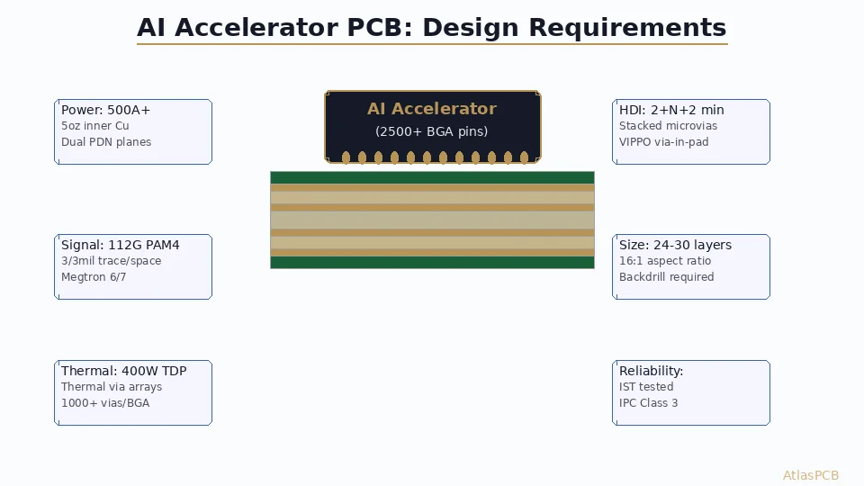
Designing PCBs for AI accelerators (NVIDIA B200-class, 800-1200W TDP) requires: (1) 20-40 layer HDI stackups with 2+ oz copper power planes for <0.5 milliohm PDN impedance, (2) Thermal via arrays under the GPU package—minimum 400 vias/cm2 with via-in-pad and copper fill for 25-40 W/cm2 heat extraction, (3) Ultra-fine pitch routing for HBM3E interfaces (0.4 mm pitch, 55 µm trace/space), and (4) Megtron 6/7 or comparable low-loss material on signal layers to support 112G PAM4 SerDes with <1 dB/inch loss at 28 GHz Nyquist frequency. Total board cost for production AI accelerator PCBs ranges from $200-800 per board depending on layer count, size, and material.
The PCB Challenge Behind the AI Revolution
Every AI chip—whether it’s NVIDIA’s B200, AMD’s MI400, or a custom Google TPU—ultimately sits on a PCB. And as AI accelerators push past 800W, 1000W, and toward 1500W thermal design power, the PCB beneath them faces engineering challenges that would have been unthinkable five years ago.
This isn’t just about “making a big board with lots of layers.” AI accelerator PCBs represent some of the most demanding designs in the electronics industry, simultaneously requiring:
- Ultra-high power delivery (1000+ amps at <1V)
- Extreme thermal management (25-40 W/cm2 heat flux through the board)
- Sub-100 µm fine features for HBM memory interfaces
- Low-loss signal integrity for 112G+ high-speed links
- All in a package that’s cost-effective enough for mass deployment
Let’s break down the engineering challenges and solutions.
Power Delivery: Getting 1000+ Amps to the Die
The Fundamental Problem
An 800W GPU operating at 0.75V core voltage draws over 1000 amperes. This current must flow from voltage regulators (VRMs) located 30-80 mm away through PCB copper planes to the BGA pads under the GPU package. The PCB’s DC resistance and AC impedance directly limit how much power the GPU can actually draw.
PCB Design Solutions
Copper weight: Minimum 2 oz (70 µm) on power planes; many designs use 3 oz (105 µm) or embedded copper slugs for critical power rail sections. Each ounce of copper on a 50 mm wide power plane reduces DC resistance by ~0.4 milliohm.
Multiple parallel power planes: Typical 28-layer AI board allocates 6-10 layers purely for power/ground:
- 3-5 power planes (split between Vcore, Vmem, Vio)
- 3-5 ground planes (essential for return current management)
Via stitching for layer transitions: Power delivery vias from VRM output to GPU BGA must handle 50-100A per via group. Design rule: minimum 20 power vias per VRM phase output, 0.35 mm drill with 0.7 mm pad, arranged in arrays.
Target PDN impedance: <0.5 milliohm flat impedance from DC to 100 MHz. This requires careful capacitor placement strategy—bulk ceramics within 5 mm of BGA edge, MLCC arrays between BGA pads using via-in-pad.
HIGH-LAYER-COUNT HDI
Up to 30-Layer Boards with Enhanced Power Delivery
We fabricate production AI accelerator PCBs with 3 oz copper planes, copper-filled vias, and Megtron 6/7 signal layers. Engineering review included.
Discuss Your Design ›
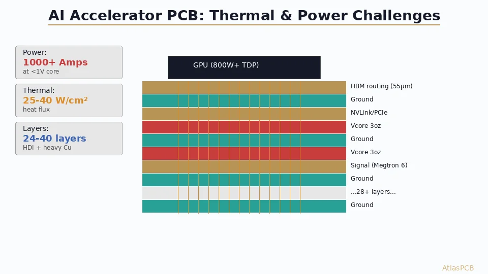
PDN Stackup Strategy
Layer 1:  Signal (HBM routing, 55 µm trace)     — 1/2 oz copper
Layer 2:  Ground (reference for L1)              — 2 oz copper
Layer 3:  Signal (NVLink / PCIe)                 — 1/2 oz copper
Layer 4:  Vcore Power                            — 3 oz copper
Layer 5:  Ground                                 — 2 oz copper
Layer 6:  Vcore Power                            — 3 oz copper
Layer 7:  Signal (high-speed, Megtron 6)         — 1/2 oz copper
Layer 8:  Ground (reference for L7)              — 2 oz copper
...
Layer 28: Ground (reference for bottom signal)   — 2 oz copper
This architecture provides <0.3 milliohm DC impedance for the Vcore rail with two dedicated 3 oz planes in parallel.
Thermal Via Design for 800W+ Packages
Heat Flux Reality
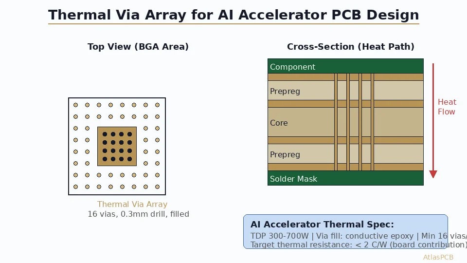
An 800W GPU in a 50x50 mm package creates 32 W/cm2 average heat flux—with hotspots exceeding 50 W/cm2 over the compute cores. While the primary thermal path is lid to TIM to heatsink, the PCB thermal path matters for:
- Junction-to-board thermal resistance (affects underside component temperatures)
- BGA solder joint thermal cycling reliability
- Supporting circuitry thermal management (VRMs generate 50-100W additional)
Thermal Via Array Design Rules
For the area directly under the GPU package:
| Parameter | Recommendation | Why |
|---|---|---|
| Via diameter | 0.3 mm | Balance between thermal conductivity and routing space |
| Via pitch | 0.6 mm | ~400 vias/cm2 provides 20+ W/cm2-K |
| Via fill | Copper-filled (via-in-pad) | Eliminates air pocket thermal resistance |
| Via depth | Full through-board | Maximum thermal path to bottom heatsink |
| Pattern | Rectangular array | Maximizes copper fill ratio |
| Annular ring | Minimum 100 µm | Ensures reliable plating and fill |
A 25x25 mm thermal via field with 0.6 mm pitch contains ~1,700 filled vias—each contributing approximately 0.003 W/K of thermal conductance through the board.
HBM Interface Routing: The Fine-Pitch Challenge
HBM3E PCB Routing Requirements
Modern AI accelerators use 4-8 stacks of HBM3E memory, each connected to the GPU via a silicon interposer or, increasingly, directly through the PCB package substrate. When HBM connects at the PCB level:
- BGA pitch: 0.4 mm (standard) or 0.3 mm (advanced)
- Required trace width: 50-65 µm
- Required space: 50-65 µm
- Impedance: 40-50 ohm single-ended, 80-100 ohm differential
- Data rate: 9.6 Gbps per pin (HBM3E)
- Pin count per stack: 1024 data + control
This demands HDI technology—specifically 2+N+2 or 3+N+3 construction with laser-drilled microvias for BGA escape routing. The microvia capture pads at 0.4 mm pitch leave only 75-100 µm routing channels between via pads.
ADVANCED HDI CAPABILITY
50 µm Trace/Space for HBM and Fine-Pitch BGA
Production-proven HDI processes for AI compute boards. Stacked microvias, via-in-pad, and impedance-controlled routing at 55 µm.
Request Capability Review ›Signal Integrity for 112G PAM4 Links
AI accelerator SerDes connections (NVLink, PCIe Gen6, proprietary interconnects) run at 112 Gbps PAM4—the most demanding signaling in production electronics:
| Parameter | Requirement | Design Impact |
|---|---|---|
| Nyquist frequency | 28 GHz | Requires Df of 0.004 or less |
| Insertion loss budget | <20 dB at 28 GHz | Limits trace length to 8-12 inches |
| Crosstalk | <-40 dB NEXT | Requires 3x spacing or ground vias |
| Impedance tolerance | +/-5% | Demands tight Dk material (+/-0.05) |
| Skew | <1 ps intra-pair | Length matching within 150 µm |
These requirements dictate:
- Material: Megtron 6 minimum; Megtron 7 or Tachyon preferred for longer reaches
- Stackup: Dedicated reference planes adjacent to every signal layer (no sharing)
- Via design: Back-drilled or blind vias to eliminate stubs
- Routing: Matched-length differential pairs with continuous reference planes
Manufacturing Reality: Who Can Build This?
Not every PCB fabricator can produce AI accelerator boards. The requirements filter for advanced capabilities:
| Capability Required | Why | Percentage of Fabs That Can |
|---|---|---|
| 28+ layer processing | Layer count | ~15% globally |
| 50 µm trace/space | HBM routing | ~10% |
| Via-in-pad copper fill | Thermal + BGA | ~20% |
| Back-drilling to +/-100 µm | Stub removal | ~25% |
| 3 oz copper processing | Power delivery | ~30% |
| Megtron 6/7 experience | Signal integrity | ~15% |
| Impedance +/-5% at 28 GHz | SerDes performance | ~10% |
The intersection of ALL requirements limits you to perhaps 5-8% of global PCB fabricators—primarily in Taiwan (Unimicron, Compeq), Japan (Ibiden, Shinko), and select advanced shops in China and Korea.
PROVEN AI BOARD FABRICATION
One of the Few Shops That Checks Every Box
Up to 30 layers, 75 µm features, 3 oz copper, Megtron 6/7, copper-filled vias, back-drill — all production-qualified under one roof.
Check Our Capabilities ›Cost Expectations
| Board Type | Layers | Size | Qty 100 Price | Qty 1000 Price |
|---|---|---|---|---|
| Training card (B200-class) | 28L | 300x400 mm | $350-500 | $200-300 |
| Inference card (compact) | 20L | 150x250 mm | $150-250 | $80-150 |
| HPC baseboard | 36L | 400x500 mm | $600-900 | $350-550 |
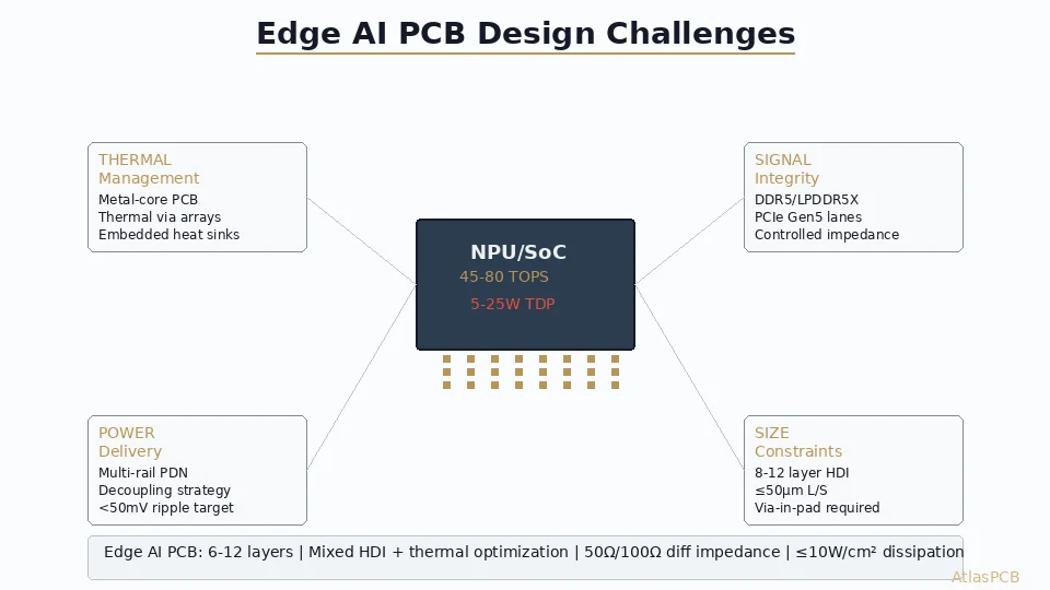
| Edge AI module | 12L HDI | 80x100 mm | $45-75 | $25-40 |
These prices reflect mid-2026 market conditions. AI PCB demand continues outpacing capacity addition, particularly for 28+ layer boards with advanced HDI features.
Designing for the Next Generation
As AI chips push toward 1500W (NVIDIA Rubin generation, 2027), PCB challenges intensify:
- Thicker copper (up to 5 oz outer, 3 oz inner) for power delivery
- More layers (40+ expected for next-gen training cards)
- Tighter features (35/35 µm trace/space for CoWoS-level integration)
- New materials (ceramic-filled substrates for thermal + electrical performance)
Engineers designing the next wave of AI hardware need fabrication partners who stay ahead of these trends.
ATLASPCB
Your AI Hardware Deserves a Fabrication Partner, Not Just a Vendor
Engineering-driven HDI fabrication for AI compute boards. 20-40+ layers, thermal optimization, power integrity review — all included.
Start Your AI Board Project ›
Related Reading:
About AtlasPCB — We specialize in complex PCB manufacturing for HDI, RF, and high-reliability applications. Explore our HDI PCB manufacturing capabilities, or get an aluminum and metal-core PCB services . Every order includes free engineering review. Get your quote.
Reviewed by AtlasPCB Engineering Team — IPC-certified manufacturing specialists with 15+ years of production experience in HDI, RF, and high-reliability PCB fabrication. Content based on factory floor data and real customer design reviews.
Frequently Asked Questions
How many PCB layers does a typical AI GPU board require?
What thermal via density is needed under an AI GPU package?
What PCB materials support 112G PAM4 signaling for AI interconnects?
- AI hardware
- GPU PCB
- thermal management
- power delivery network
- HBM
- HDI
- high-layer-count
- data center
- AI accelerator