· David Okafor · Engineering · 6 min read
PCB Fab Drawing Requirements
Your Gerber files are only half the story. Learn exactly what information your PCB fab drawing must contain to avoid misquotes, manufacturing errors, and costly respins. Includes downloadable checklist.
Quick Answer
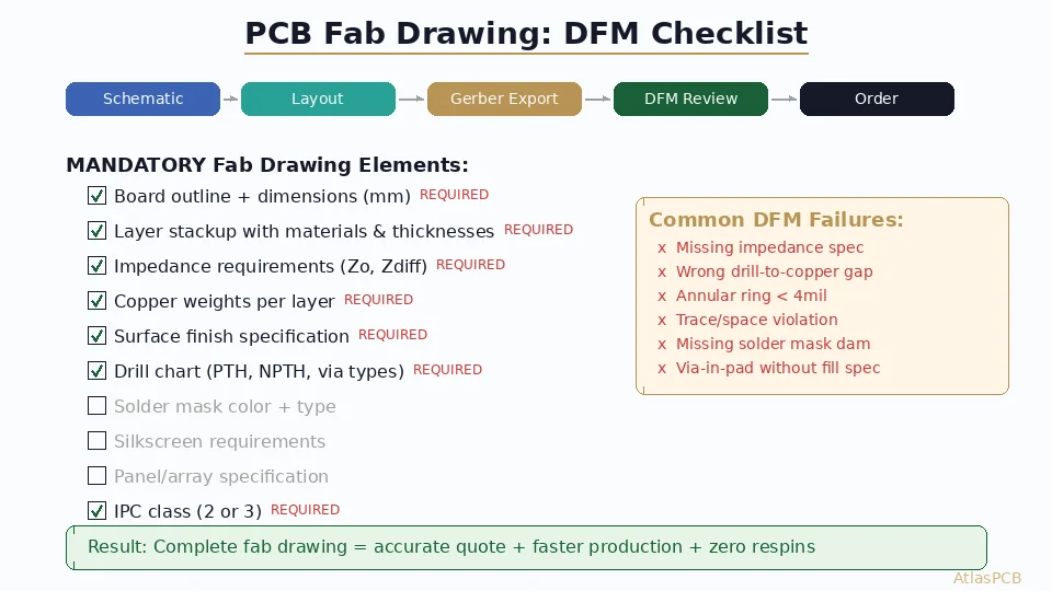
A complete PCB fab drawing must include: board outline with dimensions, full layer stackup with material callouts and thicknesses, impedance requirements per layer, copper weights, surface finish specification, drill chart distinguishing PTH/NPTH/via types, IPC class designation, and any special requirements (controlled depth drill, backdrilling, edge plating). Missing any of these forces the fabricator to assume—and assumptions cause manufacturing errors, inaccurate quotes, or project delays.
Why 60% of PCB Manufacturing Issues Trace Back to Incomplete Fab Drawings
Every PCB fabricator has the same experience: a designer uploads Gerber files, requests a quote, and the engineering team spends hours emailing back and forth to clarify missing specifications. Each question adds 1-3 days to the quote cycle. Worse, if production starts with ambiguous specs, the result is either a board that doesn’t work or an expensive respin.
The fix is simple: a complete fab drawing that answers every manufacturing question upfront. This guide covers exactly what to include.
The Mandatory 10: Information Every Fab Drawing Must Contain
1. Board Outline and Dimensions
- Overall dimensions in millimeters (or inches with mm conversion)
- Tolerances on critical dimensions (+/-0.1mm standard, +/-0.05mm if needed)
- Board thickness: target value with tolerance (e.g., 1.6mm +/-10%)
- Cutouts, slots, and routed features with dimensions
- Corner radii if specified
- Panel/array layout if ordering panelized (with V-score or tab-route callout)
2. Layer Stackup with Materials
This is the single most commonly missing element. Include:
- Number of layers
- Layer names and order (Top, GND, Signal, Power, Bottom, etc.)
- Material type per layer (FR-4 Tg170, Rogers RO4350B, polyimide, etc.)
- Dielectric thickness between each copper layer
- Copper weight per layer (specify inner and outer separately)
- Overall target thickness
Example format:
L1: Signal    | 1oz Cu  | ENIG finish
    Prepreg   | 0.2mm   | FR-4 Tg170
L2: Ground    | 0.5oz Cu|
    Core      | 0.4mm   | FR-4 Tg170
L3: Signal    | 0.5oz Cu|
    Prepreg   | 0.2mm   | FR-4 Tg170
L4: Signal    | 1oz Cu  | ENIG finish
Total: 1.6mm +/-10%
3. Impedance Requirements
For each controlled impedance trace class:
| Parameter | Example |
|---|---|
| Net class name | USB_DP/DN |
| Type | Differential pair |
| Target | 90 ohm +/-10% |
| Trace width | 4.5 mil |
| Spacing | 5.0 mil |
| Reference layers | L2 (GND) |
| Coupon required | Yes |
4. Copper Weights
- Outer layers: 1oz (35um), 2oz (70um), etc.
- Inner layers: 0.5oz, 1oz, 2oz, etc.
- Finished copper thickness after plating (outer layers gain ~25um from electroplating)
5. Surface Finish
Specify exactly one:
- HASL (lead-free or leaded)
- ENIG (with Au thickness spec: 2-4 microinches typical)
- Immersion Silver
- Immersion Tin
- OSP
- Hard Gold (specify thickness and locations)
- Selective finish (ENIG + hard gold on edge connector)
6. Drill Chart
| Hole Type | Finished Size | Tolerance | Plated? | Quantity |
|---|---|---|---|---|
| Component | 0.8mm | +/-0.05mm | PTH | 342 |
| Via | 0.3mm | +/-0.05mm | PTH | 1205 |
| Mounting | 3.2mm | +/-0.1mm | NPTH | 4 |
| Microvia L1-L2 | 0.1mm | +/-0.025mm | PTH (filled) | 89 |
Always specify:
- PTH vs NPTH
- Via fill requirements (IPC-4761 Type VII for via-in-pad)
- Aspect ratio limits (check fabricator capability)
- Back-drill requirements with target stub length
7. Solder Mask
- Color (green standard; specify if different)
- Type (LPI standard)
- Solder mask dam minimum (3mil/75um standard)
- Via tenting: tented, open, plugged, or VIPPO
- Selective areas without mask (specify in Gerber)
8. Silkscreen
- Color (white on green standard)
- Minimum line width (4mil/100um standard)
- Minimum character height (30mil/0.8mm standard)
- Reference designator requirements
9. IPC Class Designation
- Class 2: Standard electronics (consumer, commercial)
- Class 3: High reliability (aerospace, medical, military)
Class 3 adds cost (10-30%) but tightens acceptance criteria for:
- Annular ring minimum
- Copper plating thickness
- Conductor width tolerance
- Defect acceptance
10. Special Requirements
- Controlled depth drilling
- Backdrilling (specify max stub length)
- Edge plating or castellations
- Carbon ink printing
- Peelable mask areas
- Impedance test coupon requirements (specify per layer)
ELIMINATE DESIGN RESPINS
Upload Your Design for Engineering Review
Our engineers review every Gerber package for DFM issues before production. Catch problems before they become expensive mistakes.
Upload Gerber Files ›
Common DFM Failures We Catch in Review
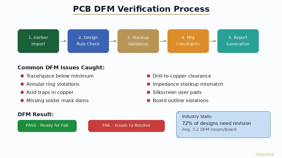
Based on thousands of designs reviewed, here are the top issues that incomplete fab drawings create:
Annular Ring Violations
Minimum annular ring for Class 2: 5mil (127um) external, 4mil (100um) internal. For Class 3: 7mil (178um) external, 5mil (127um) internal.
When drill tolerance (+/-3mil) and registration tolerance (+/-2mil) stack up, a pad that looks fine in layout can break out in production. Always verify: pad radius - (drill radius + drill tolerance + registration tolerance) >= minimum annular ring.
Via-in-Pad Without Fill Specification
Via-in-pad (VIPPO) requires the fab drawing to specify:
- Fill material (conductive or non-conductive)
- Cap plating (copper cap over fill)
- Planarity requirement (+/-10um for fine-pitch BGA)
Without this callout, the fabricator may leave vias open—causing solder wicking into the via during reflow and creating void-filled joints under BGA balls.
Missing Impedance on High-Speed Nets
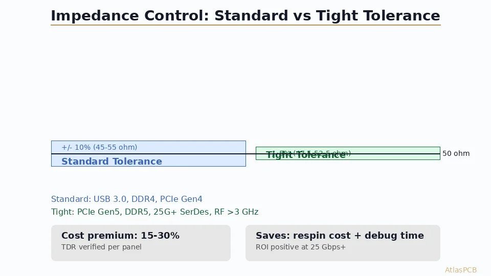
If your design has DDR4/5, PCIe Gen4/5, USB 3.x, or HDMI, you need controlled impedance. A board fabricated without impedance control on these nets will have random impedance (could be 40-70 ohm instead of target 50) and unpredictable signal integrity.
Incorrect Layer Count Assumption
A 4-layer stackup with “signal-ground-power-signal” vs “signal-ground-signal-power” has different impedance on every trace. The fab drawing must specify exact layer order and function.
DFM CONFIDENCE
Get Your Stackup Verified Before You Order
Send us your proposed stackup and impedance targets. We'll confirm manufacturability and suggest optimizations.
Fab Drawing Delivery Format
What to Include in Your Manufacturing Package
- Gerber files (RS-274X or Gerber X2): All copper layers, solder mask, silkscreen, paste, outline, drill files
- Drill files (Excellon format): Separate files for PTH, NPTH, and blind/buried vias
- Fab drawing (PDF or Gerber layer): Dimensioned drawing with all specifications
- Stackup diagram (in fab drawing or separate PDF)
- IPC netlist (IPC-D-356A): For electrical test verification
- Readme/notes (text file): Any verbal agreements or special instructions
File Naming Convention
Use clear, unambiguous names:
project-name_rev-A_top-copper.gbr
project-name_rev-A_inner-L2-gnd.gbr
project-name_rev-A_bot-copper.gbr
project-name_rev-A_top-mask.gbr
project-name_rev-A_fab-drawing.pdf
project-name_rev-A_stackup.pdf
project-name_rev-A_pth-drill.drl
project-name_rev-A_npth-drill.drl
IMPEDANCE CONTROL
Controlled Impedance PCBs with Test Coupon Verification
We provide TDR-measured impedance coupons with every controlled-impedance order. Typical tolerance: +/-5%.
View Impedance Specs ›Quick Reference Checklist
Before submitting your design for quote:
- Board dimensions and tolerances specified
- Layer stackup with materials and thicknesses documented
- Impedance requirements listed per net class
- Copper weights specified (inner and outer)
- Surface finish called out
- Complete drill chart (PTH/NPTH/via types)
- Via treatment specified (tented/open/filled/capped)
- IPC class designated
- Any backdrilling or controlled-depth drilling noted
- Panel/array requirements if applicable
- File naming clear and unambiguous
A complete fab drawing gets you: accurate quotes within 24 hours, zero engineering queries, and first-article boards that work.
ATLASPCB
Ready to Get a Fast, Accurate Quote?
Upload your Gerber package with fab drawing. Complete specs = same-day quote, no back-and-forth.
Upload and Quote ›
Related Reading:
About AtlasPCB — We specialize in complex PCB manufacturing for HDI, RF, and high-reliability applications. Explore our impedance-controlled PCB manufacturing, free engineering DFM review, or get an full PCB manufacturing capabilities . Every order includes free engineering review. Get your quote.
Reviewed by AtlasPCB Engineering Team — IPC-certified manufacturing specialists with 15+ years of production experience in HDI, RF, and high-reliability PCB fabrication. Content based on factory floor data and real customer design reviews.
Frequently Asked Questions
What's the difference between a fab drawing and a fabrication note?
Do I need to specify stackup if I just want standard FR-4?
What impedance information should the fab drawing contain?
Should I let the fabricator choose the stackup or specify it myself?
- fab drawing
- DFM
- PCB manufacturing
- Gerber files
- stackup
- impedance control
- drill chart
- IPC