· Priya Nair · Engineering · 4 min read
ENIG Surface Finish
Deep dive into ENIG (Electroless Nickel Immersion Gold) PCB surface finish. Covers deposition process, thickness specifications, black pad defect prevention, solderability testing, and comparison with HASL, OSP, and ENEPIG alternatives.
Quick Answer
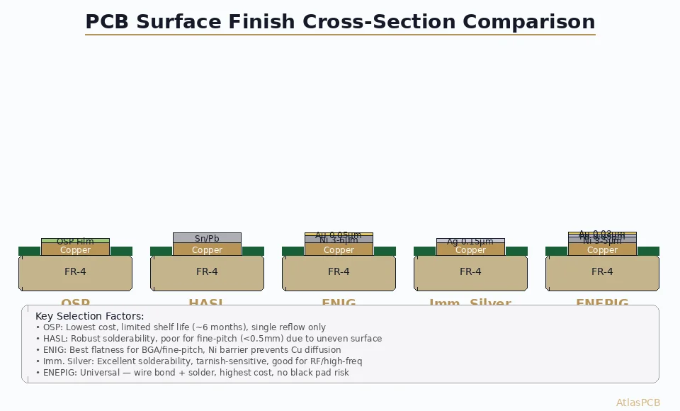
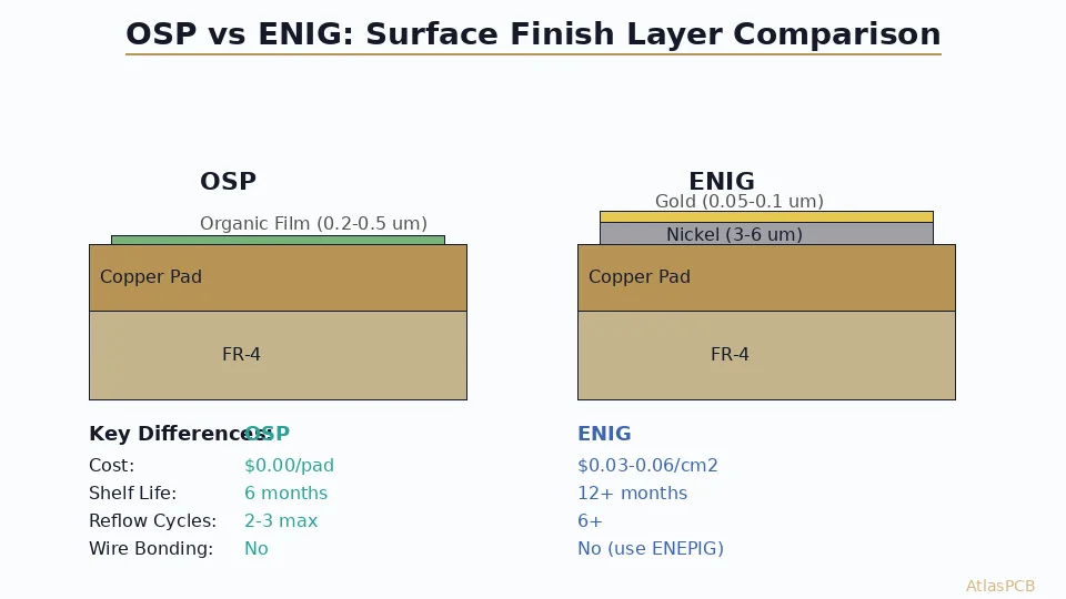
ENIG (Electroless Nickel Immersion Gold) is the most widely used high-reliability PCB surface finish, consisting of a 3–6 μm electroless nickel layer topped by 0.05–0.1 μm immersion gold. The nickel provides the solderable barrier and mechanical strength for wire bonding, while the thin gold layer protects the nickel from oxidation until assembly. ENIG offers excellent planarity for fine-pitch BGA and QFN components, 12+ month shelf life, and compatibility with lead-free soldering. The primary risk is black pad defect caused by excessive corrosion of the nickel layer during gold deposition.
ENIG Surface Finish: Process, Thickness, and Common Defects
ENIG (Electroless Nickel Immersion Gold) has become the default surface finish for complex PCBs—and for good reason. Its combination of flat pad surfaces, long shelf life, lead-free compatibility, and wire bonding capability makes it the finish of choice for BGA-intensive designs, medical devices, and any application where assembly reliability cannot be compromised.
But ENIG is also the surface finish most prone to catastrophic defects when process control slips. The infamous “black pad” failure has caused millions of dollars in field returns and has made ENIG quality one of the most important fabrication parameters to specify and verify.
The ENIG Deposition Process
Process Flow
The ENIG process consists of five chemical steps applied after solder mask development:
Cleaning/Micro-etch: Remove oxides and organic contamination from exposed copper pads. Sulfuric acid/hydrogen peroxide micro-etch creates a uniform copper surface with 1–2 μm roughness.
Activation (Catalyst): Apply palladium catalyst to initiate electroless nickel deposition. The catalyst adsorbs onto the copper surface and provides nucleation sites for nickel reduction.
Electroless Nickel Deposition: Immerse boards in nickel-phosphorus bath at 82–88°C for 20–30 minutes. The autocatalytic reaction deposits nickel-phosphorus alloy at 15–25 μm/hour. Target: 3–6 μm thickness with 7–9% phosphorus content.
Immersion Gold Deposition: Transfer to gold bath (75–85°C) for 8–15 minutes. Gold ions displace surface nickel atoms through galvanic exchange. Target: 0.05–0.10 μm gold.
Rinse and Dry: Multi-stage DI water rinse to remove residual chemicals, followed by hot air drying.
Critical Process Parameters
| Parameter | Specification | Impact of Deviation |
|---|---|---|
| Ni bath temperature | 82–88°C | Low: slow/porous deposit. High: stress cracking |
| Ni phosphorus content | 7–9% (mid-phos) | Low: poor corrosion resistance. High: poor solderability |
| Ni thickness | 3–6 μm | Low: barrier failure. High: excessive cost/stress |
| Au bath temperature | 75–85°C | Low: incomplete coverage. High: over-attack on Ni |
| Au dwell time | 8–15 minutes | Short: pinholes. Long: black pad risk |
| Au thickness | 0.05–0.10 μm | Low: Ni oxidation. High: gold embrittlement in solder |
ENIG vs Other Surface Finishes
| Property | ENIG | HASL | OSP | ENEPIG | Imm. Silver |
|---|---|---|---|---|---|
| Planarity | Excellent | Poor | Excellent | Excellent | Excellent |
| Shelf life | 12+ months | 12+ months | 6 months | 12+ months | 6–12 months |
| Lead-free compatible | Yes | Lead-free HASL only | Yes | Yes | Yes |
| Wire bondable | Au wire only | No | No | Au and Al wire | No |
| Fine pitch (≤0.5mm) | Yes | No | Yes | Yes | Yes |
| Cost (relative) | 1.0× | 0.5× | 0.3× | 1.5× | 0.7× |
| Black pad risk | Moderate | None | None | Very low | None |
| Multiple reflow cycles | 3–5 | 5+ | 2–3 | 5+ | 3–4 |
For a comprehensive comparison, see our [PCB surface finish comparison guide]/blog/pcb-surface-finish-comparison-2026/).
Black Pad Defect: Identification and Prevention
What Is Black Pad?
Black pad (also called “black nickel”) is a solderability failure specific to ENIG. During gold deposition, the galvanic exchange reaction attacks nickel grain boundaries, creating a phosphorus-enriched, oxidized layer that solder cannot wet. The defect is invisible until assembly—joints appear normal but have zero mechanical strength and fail under any stress.
Root Causes
- Nickel grain structure: Columnar grain structure (from low-phosphorus nickel) exposes more grain boundary area to gold attack
- Excessive gold bath activity: Over-concentrated or high-temperature gold bath accelerates nickel corrosion
- Nickel bath contamination: Copper drag-in or organic contamination creates non-uniform nickel with vulnerable zones
- Extended gold immersion time: Longer dwell = more nickel dissolution = thicker corroded layer
Prevention Checklist
- Maintain nickel phosphorus content at 7–9% (mid-phos) — tested weekly by XRF
- Control gold bath temperature within ±2°C of target
- Limit gold immersion time to manufacturer specification
- Monitor nickel bath loading (MTO — metal turnovers) and dump/replenish on schedule
- Implement incoming QC: cross-section 2 pads per panel, inspect Ni-Au interface at 500×
Quality Verification Methods
XRF Measurement
X-ray fluorescence (XRF) is the standard non-destructive method for verifying ENIG thickness:
| Measurement | Specification | Frequency |
|---|---|---|
| Gold thickness | 0.05–0.10 μm | Every panel, 5 points |
| Nickel thickness | 3.0–6.0 μm | Every panel, 5 points |
| Phosphorus % | 7–9% | Weekly per bath |
Cross-Section Analysis
Microsectioning per IPC-TM-650 2.2.1 reveals:
- Nickel grain structure (amorphous preferred over columnar)
- Nickel-gold interface integrity (no corrosion layer)
- Nickel-copper interface bonding
- Actual thickness vs XRF readings
Solderability Testing
| Test Method | Standard | Pass Criteria |
|---|---|---|
| Wetting balance | IPC J-STD-003 | >2mN/mm force, <1 sec wetting time |
| Solder spread | IPC-TM-650 2.4.45 | >80% pad coverage |
| Steam aging | IPC J-STD-003 | Passes after 8 hours steam |
When to Upgrade to ENEPIG
Consider upgrading from ENIG to [ENEPIG]/blog/enepig-vs-enig/) when:
- Both gold wire bonding and aluminum wire bonding are needed on the same board
- Zero tolerance for black pad defect (the palladium barrier layer in ENEPIG eliminates the failure mechanism)
- The application is medical or aerospace where field failure is not acceptable
- [BGA pad reliability]/blog/pcb-pad-design-bga-qfn/) must be guaranteed through 5+ reflow cycles
Ready to discuss surface finish options? Upload your Gerbers for finish recommendation and quote.
Further Reading
- [PCB Surface Finish Guide: HASL vs ENIG vs ENEPIG vs OSP]/blog/pcb-surface-finish-comparison-2026/)
- [ENEPIG vs ENIG: When to Choose the Premium Finish]/blog/enepig-vs-enig/)
- [PCB Pad Design for BGA and QFN]/blog/pcb-pad-design-bga-qfn/)
About AtlasPCB — We specialize in complex PCB manufacturing for HDI, RF, and high-reliability applications. Explore our RF and high-frequency PCB services, or get an full PCB manufacturing capabilities . Every order includes free engineering review. Get your quote.
Reviewed by AtlasPCB Engineering Team — IPC-certified manufacturing specialists with 15+ years of production experience in HDI, RF, and high-reliability PCB fabrication. Content based on factory floor data and real customer design reviews.
Frequently Asked Questions
What are the standard ENIG thickness requirements?
What causes black pad defect in ENIG?
When should I choose ENIG over HASL or OSP?
- surface-finish
- enig
- pcb-manufacturing
- solderability