· David Okafor · Engineering · 10 min read
PCB DFM Check: Pre Order
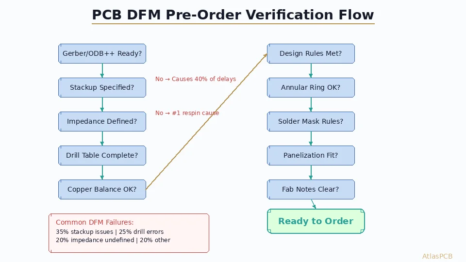
A systematic DFM verification checklist covering the specific items that cause fabrication holds, requotes, and delivery delays. Based on real data from 10,000+ orders — these are the issues manufacturers actually encounter, not theoretical possibilities.
Quick Answer
The top 5 DFM issues causing fabrication delays are: missing or ambiguous stackup specification (28% of holds), undefined impedance requirements on high-speed nets (22%), drill-to-copper clearance violations (18%), incomplete fab notes regarding surface finish or special requirements (15%), and annular ring violations on high-density BGA breakouts (12%). A systematic pre-order check covering these items eliminates 80% of the back-and-forth that delays your boards by 3-7 days.
The Real DFM Failure Data
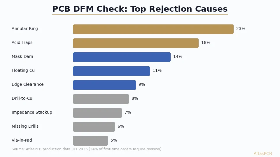
We track every fabrication hold in our system. Across 10,000+ orders processed in the last 12 months, the distribution of DFM issues that cause holds is remarkably consistent:
| Issue Category | % of Holds | Typical Delay Added | Preventable? |
|---|---|---|---|
| Missing/ambiguous stackup | 28% | 3-5 days | Yes |
| Undefined impedance | 22% | 2-4 days | Yes |
| Drill-to-copper violation | 18% | 1-3 days | Yes |
| Incomplete fab notes | 15% | 2-3 days | Yes |
| Annular ring violation | 12% | 1-2 days | Yes |
| Other (artwork, silkscreen) | 5% | 1 day | Mostly |
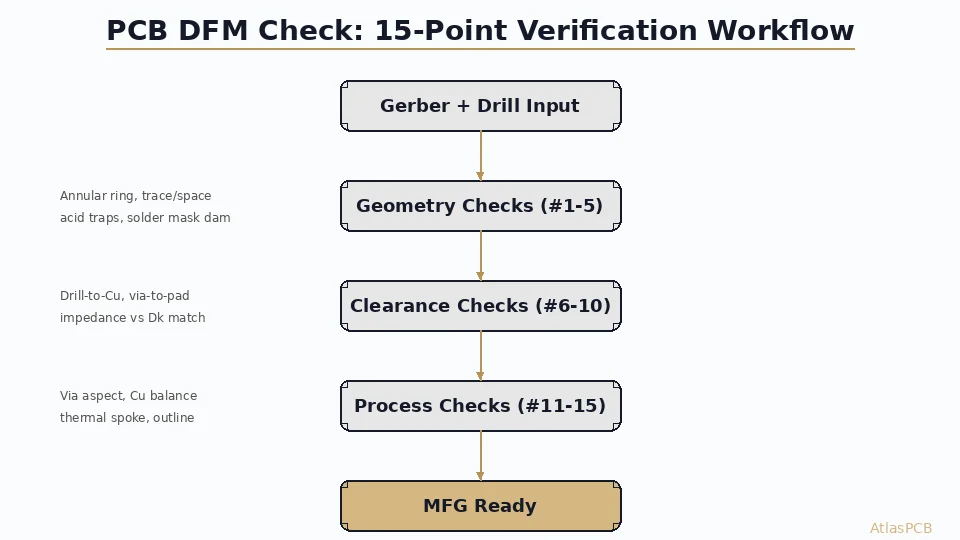
The striking finding: 95% of holds are preventable with a 15-minute pre-submission check. The rest of this guide covers exactly what to verify.
Check 1: Stackup Specification
This is the single most impactful DFM check because it affects everything downstream — impedance, cost, lead time, and material procurement.
Your stackup document must answer these questions unambiguously: How many layers? What material (standard FR-4, high-Tg, Rogers, polyimide)? What copper weight on each layer? What is the target finished thickness? Are there specific dielectric thickness requirements between any layers?
The common failure mode: an engineer submits 8-layer Gerber files with no stackup document, assuming “standard” material. But their simulation requires 4mil dielectric between layers 3 and 4 for impedance, while our standard 8-layer stackup uses 7.6mil dielectric in that position. Without the stackup document, we fabricate to standard spec — and the board fails impedance. With the document, we catch the discrepancy before pressing.
In our facility, we see this issue most frequently with designs crossing the 4-to-6 and 6-to-8 layer boundary, where designers upgrade layer count for the first time and do not realize that stackup specification becomes critical above 4 layers.
STACKUP SUPPORT
Not Sure About Your Stackup? We Help You Define It
Upload your design with target impedance requirements — our stackup engineering team proposes a manufacturable configuration with material selection and tolerance analysis.
Get Stackup Recommendation ›
Check 2: Impedance Requirements
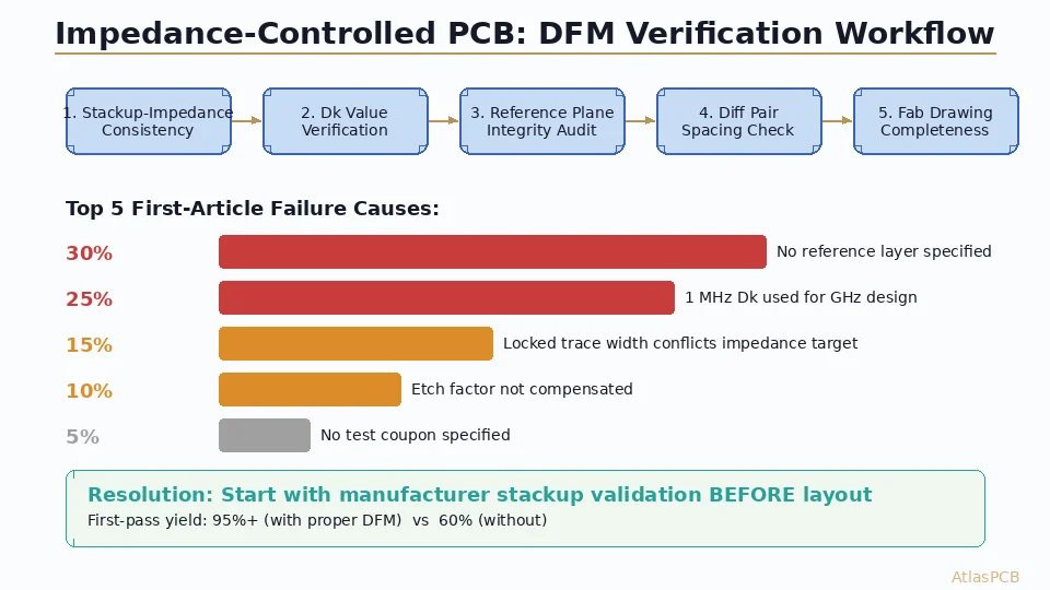
If your design has any controlled-impedance traces, the fab drawing must specify: target impedance value, tolerance (±5%, ±7%, ±10%), which layers, and which reference plane. “50 ohm” written somewhere on the fab drawing is not sufficient.
The information gap we encounter most frequently is the reference plane ambiguity. In a 6-layer stackup (Sig-GND-Sig-Sig-GND-Sig), Layer 1 traces reference Layer 2 (ground). But what does Layer 3 reference — Layer 2 above it or Layer 5 below? The impedance is different depending on the reference, and your EDA tool’s impedance calculator made an assumption that may not match what we build.
Specify impedance like this: “Layer 1: 50 ohm single-ended ±5%, referenced to Layer 2 (GND). Layer 3: 100 ohm differential ±5%, referenced to Layer 2 (GND). Layer 6: 50 ohm single-ended ±7%, referenced to Layer 5 (GND).”
Check 3: Drill-to-Copper Clearance
Drill-to-copper clearance violations are the third most common DFM issue and one of the most dangerous because they can create intermittent shorts that only appear after thermal cycling in the field.
The minimum clearance between a drilled hole wall and the nearest copper feature on internal layers depends on the manufacturer’s registration capability. For standard multilayer (4-8 layers), most manufacturers require 8mil minimum clearance from hole edge to nearest internal copper. For high layer count (12+) or HDI, this may increase to 10mil due to registration stack-up.
The common failure pattern: a designer places a via adjacent to a trace on an internal layer with only 5mil clearance. The EDA tool shows this as acceptable because the software uses the drill center-to-copper distance, not the hole edge-to-copper distance. After drilling (with ±3mil positional tolerance) and plating (adding 1mil to hole diameter), the actual clearance becomes 1-2mil — within the electrical breakdown range under humidity.
Quick check: In your EDA tool, set the non-functional pad clearance to at least 8mil from hole edge. Run DRC. Any violations need attention before ordering.
Check 4: Fab Notes Completeness
Incomplete fab notes force the manufacturer to assume — and assumptions create risk. Every order should specify these minimum items:
Material: “FR-4” is not specific enough for boards above 4 layers. Specify: FR-4, Tg ≥ 170°C (e.g., IT180A, EM827). If Tg doesn’t matter, say so: “Standard Tg FR-4 acceptable.”
Copper weight: Specify per-layer if different. “1oz outer, 0.5oz inner” is clear. Just “1oz” leaves inner layers ambiguous.
Surface finish: ENIG, HASL (lead-free or leaded), OSP, Immersion Tin, Immersion Silver. Do not leave blank — each has different pad geometry requirements.
Special processes: Via-in-pad (must specify filled + planarized), carbon ink, peelable solder mask, edge plating, controlled depth drilling. Omitting these from fab notes means they will not be quoted or performed.
DFM REVIEW
Catch Issues Before Fabrication — Not During
Our DFM engineering team reviews every order for manufacturability before production begins. We flag issues and propose solutions rather than building boards we know will have problems.
Submit for DFM Review ›Check 5: Annular Ring
Annular ring is the copper remaining around a drilled hole after drilling and registration. Minimum annular ring for IPC Class 2 is 5mil (external) and 4mil (internal). IPC Class 3 requires 5mil on all layers.
The problem emerges on BGA breakout patterns where pad sizes are minimized to fit routing channels between pads. A 0.8mm-pitch BGA with 12mil drill and 20mil pad leaves 4mil annular ring — exactly at the Class 2 limit. Add 2-3mil drill registration tolerance and you are below minimum on internal layers.
For HDI designs with microvias, the calculation is different. Laser-drilled microvias (typically 4mil/100μm drill) in 10mil pads have 3mil annular ring per side. This is acceptable because laser drilling has ±0.5mil positional accuracy versus ±3mil for mechanical drilling. But your DRC rules must distinguish between via types.
Our DFM check specifically flags annular ring violations that fall between 3-5mil — the danger zone where the board will be fabricated but may have reliability issues in thermal cycling. These are the violations most EDA tools will not flag if using default rule settings.
Check 6: Copper Balance
Unbalanced copper distribution between layers causes board warping during lamination and reflow. This is particularly problematic for thin boards (<1.0mm) and high layer counts (>8 layers) where the total copper area asymmetry creates significant mechanical stress.
The check: compare copper fill percentage between symmetric layer pairs (Layer 1 vs Layer N, Layer 2 vs Layer N-1, etc.). If any pair differs by more than 20% in copper area, warping risk increases significantly. For boards going through multiple reflow cycles (double-sided SMT assembly), this threshold drops to 15%.
The common failure: a designer places a large ground pour on one outer layer and leaves the other with minimal copper (just traces and pads). After reflow, the board bows 2-3mm — exceeding IPC-A-600 limits for flatness. Adding copper thieving (non-functional copper patterns) to the bare side balances the stackup and prevents warping.
Check 7: Solder Mask Design Rules
Solder mask between pads (the “web” width) is frequently violated on fine-pitch designs. Minimum solder mask web width varies by manufacturer: typically 3mil (75μm) for LPI solder mask. Below this, the mask strip between pads peels during processing and causes solder bridging in assembly.
For 0.4mm-pitch QFN packages with 8mil pads and 8mil gaps: the solder mask opening is typically solder-mask-defined (SMD) at 1-2mil per side smaller than the copper pad. This leaves a 4-6mil mask web between openings — usually acceptable. But 0.3mm-pitch CSP packages often violate minimum web rules, requiring mask design modification or acceptance of potential bridging risk.
Check 8: Drill Table Completeness
Your drill file must include every hole size in the design with clear designation: plated versus non-plated, mechanical versus component, and tolerance class. A common issue: mounting holes specified as plated when they should be non-plated (or vice versa), and press-fit holes requiring ±0.5mil tolerance not flagged as such.
Verify: export your drill table and confirm each hole size matches your component requirements. Pay special attention to any holes requiring tolerance tighter than ±3mil (standard) — these must be explicitly called out in fab notes.
Check 9: Panel Utilization (Cost Impact)
While not a “pass/fail” DFM check, board dimensions that optimize panel utilization significantly affect cost. Standard panel sizes for prototype are 18”×24” (working area approximately 16”×22”). Boards that fit the panel efficiently with 8mil routing gaps between units cost 15-30% less per unit than boards requiring custom panelization.
The quick math: a 50×50mm board fits 7×11 = 77 units per panel. A 55×55mm board fits 6×10 = 60 units — 22% fewer boards per panel, directly increasing per-unit cost. If you have dimensional flexibility, rounding down to the nearest 5mm increment that fits more units per panel is free cost optimization.
PANELIZATION
Panel Layout Optimization Included in Every Quote
We propose optimal panelization for your board dimensions — maximizing utilization and minimizing per-unit cost. V-score, tab-route, or breakaway options based on your assembly needs.
Get Optimized Quote ›Check 10: Via-in-Pad Specification
If your design uses via-in-pad (common for BGA breakout), you must explicitly specify “filled and planarized” in fab notes. Simply having vias placed in pads in your Gerber data does not tell the manufacturer how to process them.
Unfilled via-in-pad causes solder wicking during assembly — solder flows down the via barrel instead of forming a proper BGA joint. This creates open circuits on the BGA that are invisible to optical inspection and only caught by X-ray or functional testing.
The spec language should be: “All vias in BGA pad areas: filled with non-conductive epoxy, planarized to ±0.5mil of surrounding copper, and capped with copper plating.” This adds $0.50-2.00 per board at prototype quantity but prevents assembly failures that cost hundreds in debug time.
ATLASPCB
Ready to Order? Submit Your Design With Confidence
Run through this checklist, then upload your Gerber files. Our engineering team performs DFM review on every order — catching any remaining issues before fabrication begins. No surprises, no delays.
Upload Design for Quote ›
Reviewed by AtlasPCB Engineering Team — 15+ years in advanced PCB fabrication for RF, HDI, and rigid-flex applications.
Related Reading:
About AtlasPCB — We specialize in complex PCB manufacturing for HDI, RF, and high-reliability applications. Explore our impedance-controlled PCB manufacturing, free engineering DFM review, or get an full PCB manufacturing capabilities . Every order includes free engineering review. Get your quote.
Reviewed by AtlasPCB Engineering Team — IPC-certified manufacturing specialists with 15+ years of production experience in HDI, RF, and high-reliability PCB fabrication. Content based on factory floor data and real customer design reviews.
Frequently Asked Questions
What is the most common PCB DFM issue that delays orders?
How long does a DFM hold typically delay my PCB order?
Should I run DFM checks myself or rely on the manufacturer?
What DFM rules differ between a standard and HDI PCB?
What information should my fab notes include?
- PCB DFM check
- design for manufacturability PCB
- PCB manufacturing
- impedance controlled PCB
- PCB stackup design guide