· Sophia Reyes · Engineering · 9 min read
Impedance Controlled PCB
Not every board needs tight impedance control. This guide explains exactly where the ±10% vs ±5% tolerance boundary lies, what manufacturing processes create the difference, and how to specify impedance requirements without over-engineering or under-specifying your design.
Quick Answer
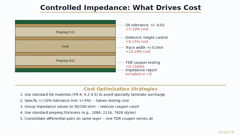
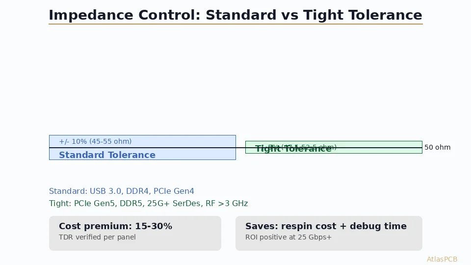
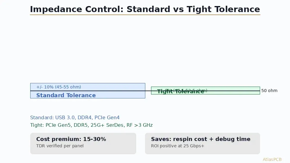
Standard PCB fabrication delivers ±10% impedance tolerance without special processing. Tight ±5% tolerance requires stackup simulation with actual material Dk data, etch compensation calibration, and TDR verification on every panel — processes that add 15-30% to board cost. The crossover point where tight tolerance becomes mandatory is approximately 5 Gbps for single-ended and 10 Gbps for differential signaling, though it depends on trace length and loss budget.
The 30-Second Decision
| Your Fastest Signal | Standard ±10% | Tight ±5% | Notes |
|---|---|---|---|
| SPI/I2C (<100 MHz) | Sufficient | Overkill | Save the cost |
| USB 2.0 (480 Mbps) | Sufficient | Optional | Only if trace >6” |
| Gigabit Ethernet | Acceptable | Recommended | Depends on connector quality |
| USB 3.2 Gen 2 (10G) | Marginal | Required | Return loss will fail |
| PCIe Gen 4 (16 GT/s) | Fails | Required | Plus low-loss dielectric |
| PCIe Gen 5 (32 GT/s) | Fails | Minimum | Need ±3% or better |
| 25G/56G Ethernet | Fails | Tight minimum | Material Dk tolerance matters too |
If your fastest interface is below the bold line — standard fabrication works. Above it, you need an impedance-controlled PCB manufacturer with TDR verification capability.
What Creates the Tolerance Difference
The impedance of a PCB trace depends on four physical parameters: trace width, dielectric thickness, dielectric constant (Dk), and copper thickness. Manufacturing variation in any of these affects final impedance. The difference between ±10% and ±5% comes down to how tightly the manufacturer controls each parameter.
Standard fabrication uses catalog Dk values for impedance calculation (if they calculate at all), applies a generic etch factor based on copper weight, and presses the laminate at standard parameters without adjusting for specific dielectric thickness targets. Each parameter varies within its natural process window, and those variations compound multiplicatively.
In our production data from the past quarter, standard-process boards show impedance distribution with a standard deviation of approximately 3.5% — meaning ±10% captures the 3-sigma range. This is perfectly acceptable for the majority of PCB applications. The boards are not “bad” — they are simply not optimized for impedance.
Tight tolerance production starts differently. Before fabrication begins, our process engineering team simulates the stackup using measured Dk data from the actual material lot we will press your boards with. Rogers publishes Dk to two decimal places, but actual pressed values vary by ±0.03 between lots — at 10 GHz, this alone creates 1-2% impedance variation. By measuring the specific material, we eliminate this variable.
IMPEDANCE CONTROL
±5% Impedance with TDR Data on Every Panel
Pre-production stackup simulation with actual material Dk, etch compensation specific to your geometry, and TDR verification shipped with every order.

The Etch Compensation Problem
Etch compensation is where most impedance failures originate, and it is also where the difference between a capable impedance-controlled PCB manufacturer and a standard shop becomes most apparent.
When copper is etched, the chemical process removes material laterally as well as vertically. A trace designed at 5.0mil will etch to approximately 4.2-4.5mil depending on copper weight, resist type, and chemistry freshness. This etch bias must be compensated in the artwork — designing the trace wider so it etches to the target width.
Standard shops apply a fixed etch compensation value: typically +0.5mil for 0.5oz copper, +1.0mil for 1oz, +1.5mil for 2oz. This generic approach works within ±10% because the etch bias is roughly predictable. But “roughly” is not sufficient for tight tolerance.
A controlled-impedance manufacturer characterizes their actual etch bias weekly, broken down by copper weight, panel position (edges etch more than centers), and bath chemistry age. In our facility, we measure etch coupons at the start of each production shift and adjust compensation accordingly. The difference between a fresh chemistry bath and one approaching change-out can shift etch bias by 0.3mil — enough to move impedance by 3-4% on fine traces.
For boards requiring tight impedance control, we also account for panel position effects. Outer traces on a panel experience more aggressive etching due to fresh chemistry flow, while inner traces see slightly depleted chemistry. This positional variation can create 2-3% impedance spread across a single panel. Addressing it requires compensating artwork differently based on trace position relative to panel edges — something no standard shop does because it requires custom CAM engineering for each job.
When to Specify — And When Not To
Over-specifying impedance control wastes money. Under-specifying causes signal integrity failures. The engineering question is where your design actually sits on this spectrum.
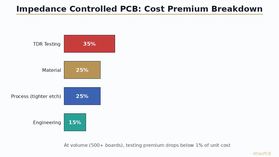
Consider a typical IoT device with a STM32 microcontroller, SPI flash, I2C sensors, and a WiFi module. The SPI bus runs at 50 MHz with 2-inch traces, I2C runs at 400 KHz over 1 inch, and the WiFi module has a 50-ohm RF trace to the antenna. In this design, only the RF trace needs impedance control — the SPI and I2C traces will function perfectly with standard ±10% tolerance. Specifying impedance control on the entire board adds 20% to cost with zero functional benefit.
Conversely, a network switch PCB with 10G SerDes channels, DDR4 memory interfaces, and PCIe Gen 4 backplane connections needs tight impedance control on virtually every signal layer. The return loss specification for 10G SFP+ channels requires ±5% impedance consistency across 8+ inch trace runs — standard fabrication cannot achieve this reliably.
The practical guideline from our engineering team: if your design simulation shows less than 1 dB return loss margin at your operating frequency with ±5% impedance, you need controlled impedance. If your simulation shows 3+ dB margin with ±10%, standard fabrication saves cost without risk.
STACKUP ENGINEERING
Not Sure If You Need Impedance Control?
Upload your design — our signal integrity team reviews your stackup and advises whether controlled impedance is necessary for your specific interfaces and trace lengths.
Get Stackup Recommendation ›How to Specify Impedance in Your Fab Drawing
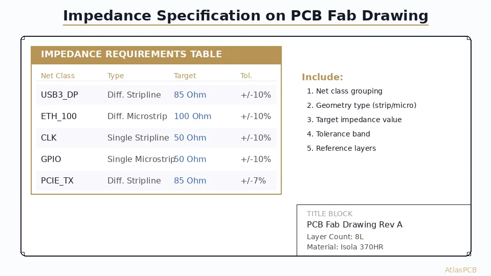
Effective impedance specification requires four elements that many designers omit, leading to manufacturer guesswork and potential failures:
1. Target impedance and tolerance for each controlled net class. Do not simply write “50 ohm ±10%.” Specify: “Differential 100 ohm ±5% for USB 3.2 pairs on Layers 1/8, Single-ended 50 ohm ±7% for RGMII traces on Layer 3.” This tells the manufacturer exactly which traces need which level of control.
2. Reference plane identification. Impedance depends on the distance to the reference ground plane. If your stackup has signal layers referenced to different planes, specify which plane is the impedance reference for each controlled layer. A common failure: the designer assumes Layer 3 references Layer 2 (ground), but the manufacturer interprets it as referencing Layer 4 (power) — completely different impedance.
3. Stackup constraints that affect impedance. If your design assumes specific dielectric thickness (e.g., 4mil core between signal and ground), state this explicitly. Many manufacturers will adjust dielectric thickness to optimize panel cost unless constrained, potentially shifting your impedance.
4. Copper roughness specification. At frequencies above 5 GHz, copper surface roughness affects both impedance and insertion loss. Standard ED copper (Rz ~6μm) versus low-profile (Rz ~3μm) versus hyper-low-profile (Rz ~1.5μm) creates measurable impedance differences at high frequency. If your simulation assumes specific roughness, specify it.
Cost Optimization: Getting Tight Tolerance Where It Matters
The most cost-effective approach for mixed-signal designs is selective impedance control. Here is how to structure your specification to get tight tolerance where necessary without paying for it everywhere:
Identify which layers carry speed-critical signals and specify ±5% only on those layers. For a typical 8-layer board with high-speed signals on layers 1, 3, 6, and 8, with power distribution on layers 4/5 and low-speed signals on layer 2/7, you only need impedance control on 4 of 8 layers.
Within controlled layers, distinguish between nets that truly need ±5% versus those where ±7% suffices. PCIe Gen 4 differential pairs need ±5%. RGMII at 125 MHz might be fine at ±7%. This distinction affects whether the manufacturer needs to run TDR on additional coupons.
Consider hybrid stackups where different dielectric materials serve different purposes. Standard FR-4 for power planes and low-speed signals, with mid-Tg or Megtron on high-speed signal layers. This optimizes cost while maintaining performance where it matters.
COST OPTIMIZATION
Selective Impedance Control — Pay Only Where Needed
Our quoting system supports per-layer impedance specification. Get tight tolerance on critical signal layers and standard processing elsewhere — optimizing cost without compromising performance.
Upload Design for Quote ›Verification: What Your TDR Report Should Show
When you receive boards from an impedance-controlled PCB manufacturer, the TDR report should contain:
- Target impedance for each coupon (matched to your specification)
- Measured impedance with measurement uncertainty stated
- Pass/fail against your specified tolerance
- Coupon location on panel (identifies if positional variation exists)
- Date, instrument model, and calibration status
If a manufacturer provides impedance “data” without coupon identification or instrument details, the numbers are likely calculated from process parameters rather than actually measured. Calculated impedance is useful for pre-production estimation but does not replace post-fabrication TDR verification.
In our production process, every panel containing impedance-controlled boards gets TDR tested against the customer’s specification before boards are routed from the panel. Panels failing impedance are scrapped and re-manufactured — not shipped with a note. This is the difference between “impedance controlled” as a process commitment versus “impedance controlled” as a checkbox on a quote form.
ATLASPCB
Impedance-Controlled PCB Manufacturing — Verified, Not Estimated
±5% tolerance with TDR verification on every production panel. Pre-production stackup simulation. Full impedance report included in shipment. 1-30 layers, FR-4 through Rogers.
Get Impedance-Controlled Quote ›
Reviewed by AtlasPCB Engineering Team — 15+ years in advanced PCB fabrication for RF, HDI, and rigid-flex applications.
Related Reading:
About AtlasPCB — We specialize in complex PCB manufacturing for HDI, RF, and high-reliability applications. Explore our impedance-controlled PCB manufacturing, or get an full PCB manufacturing capabilities . Every order includes free engineering review. Get your quote.
Reviewed by AtlasPCB Engineering Team — IPC-certified manufacturing specialists with 15+ years of production experience in HDI, RF, and high-reliability PCB fabrication. Content based on factory floor data and real customer design reviews.
Frequently Asked Questions
What impedance tolerance does a standard PCB fab house deliver?
How much more does ±5% impedance control cost versus standard?
At what data rate do I need tight impedance control?
How does a manufacturer achieve ±5% impedance tolerance?
Can I mix controlled and uncontrolled impedance on the same board?
- impedance controlled PCB manufacturer
- impedance control
- PCB stackup design guide
- signal integrity
- PCB manufacturing