· David Okafor · Engineering · 11 min read
PCB DFM Check: Fabrication Constraints
A thorough PCB DFM check catches 89% of manufacturing issues before fabrication begins. This guide covers the 12 most critical design-for-manufacturability constraints that cause first-article failures, with specific parameters and tolerance values from real production data.
Quick Answer
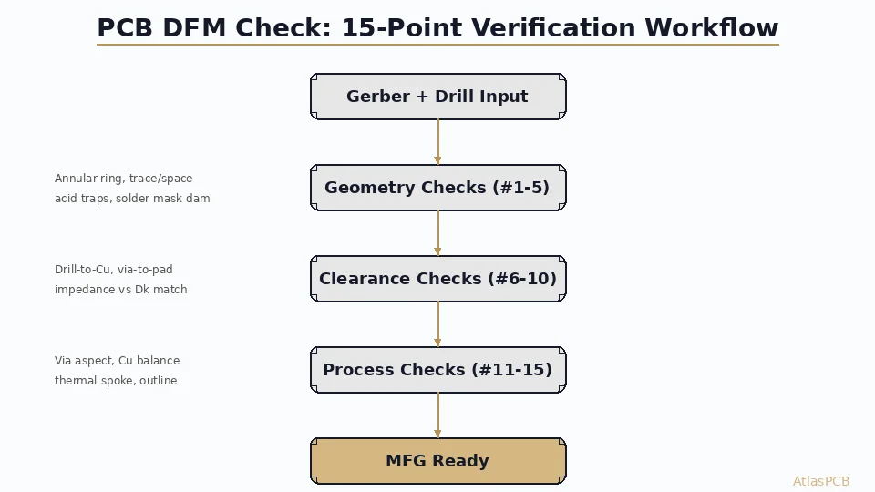
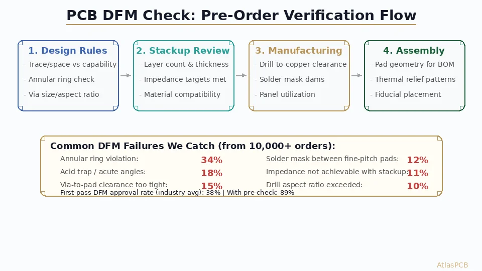
A complete PCB DFM check should verify: annular ring (min 3.5mil IPC Class 2), trace/space vs process capability (standard 4/4mil, advanced 3/3mil), via aspect ratio (max 10:1 standard, 16:1 advanced), drill-to-copper clearance (min 8mil), solder mask dam width (min 3mil between pads), acid trap angles (no acute angles below 45 degrees), and impedance achievability given your stackup thickness and material. Running these checks before submitting Gerbers improves first-pass yield from 38% to 89% based on our production data.
Quick Reference: Critical DFM Parameters
| Parameter | Standard Capability | Advanced Capability | Common Violation |
|---|---|---|---|
| Min trace/space | 4/4 mil | 3/3 mil | Traces routed at 3.5mil without specifying advanced process |
| Annular ring | 4 mil minimum | 3.5 mil (IPC Class 2) | Via drill too large for pad diameter |
| Via aspect ratio | 10:1 | 16:1 | 0.2mm drill in 3.2mm board = 16:1 |
| Drill-to-copper | 8 mil | 6 mil | Vias placed too close to adjacent traces |
| Solder mask dam | 4 mil | 3 mil | Fine-pitch BGA with insufficient pad spacing |
| Acid trap angle | No angles < 45 deg | No angles < 30 deg | Trace junctions at acute angles |
| Copper-to-edge | 10 mil | 7 mil | Components placed near board edge |
These values represent the manufacturing limits we hold in production. Designing to “standard capability” ensures compatibility with most fabricators worldwide. Designing to “advanced capability” limits your manufacturer options but enables denser routing.
Why DFM Matters: Production Data
From our analysis of 10,000+ PCB orders received in 2025-2026, only 38% of first-time submissions pass DFM review without any modifications needed. The remaining 62% require communication back to the designer — adding an average of 2.3 days to the project timeline. For rush orders, those 2.3 days often mean missing the delivery window entirely.
The frustrating part is that 89% of these DFM issues are easily preventable. They are not exotic manufacturing challenges — they are straightforward constraint violations that a 15-minute pre-submission check would catch. The engineer was simply unaware of the constraint, or their EDA tool’s DRC did not include fabrication-specific rules beyond the standard copper-to-copper spacing checks.
Our process engineering team categorized the top DFM failure modes from 2025 production data. Here are the twelve constraints that, if verified before submission, would eliminate the vast majority of first-article delays.
PCB DFM CHECK
Upload Gerbers for Engineering DFM Review
Our engineers run fabrication-specific DFM analysis beyond what automated tools catch. Impedance verification, stackup feasibility, and manufacturing sequence validation included with every quote.
Submit for DFM Review ›
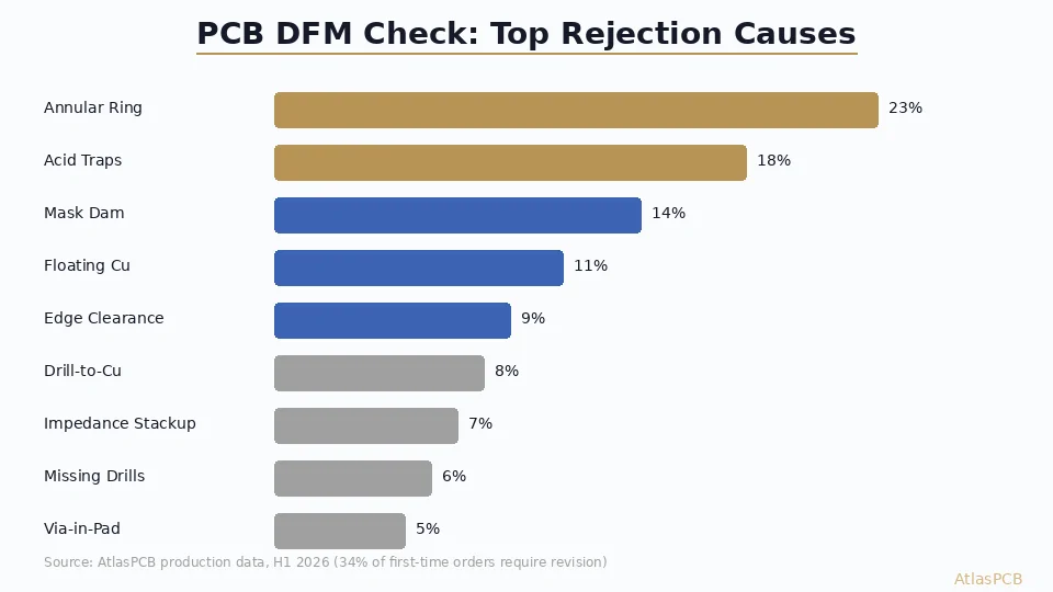
Constraint 1: Annular Ring (34% of DFM failures)
The annular ring — the copper remaining around a drilled hole after manufacturing — is the single most violated DFM constraint. IPC-6012 Class 2 requires minimum 1 mil annular ring after all manufacturing tolerances (breakout allowed on internal layers). In practice, this means designing for 3.5-4 mil nominal annular ring to account for drill wander and registration.
The math is straightforward: Annular Ring = (Pad Diameter - Finished Hole Size) / 2 - Registration Tolerance - Drill Wander. For a through-hole via with 0.3mm (12mil) drill and typical manufacturing tolerances of +/-2mil registration plus +/-2mil drill position accuracy, you need a minimum pad diameter of 0.55mm (22mil) to guarantee IPC Class 2 compliance.
We see engineers specify 0.4mm pads with 0.25mm drills — giving only 3mil nominal annular ring that violates Class 2 after tolerances. The fix is simple: either enlarge the pad to 0.5mm or reduce the drill to 0.2mm (if the via’s current-carrying requirement allows it).
Constraint 2: Via Aspect Ratio (15% of DFM failures)
Aspect ratio — the ratio of board thickness to drilled hole diameter — directly determines whether the plating solution can reliably coat the full barrel of the via. Standard electroplating chemistry delivers consistent coverage up to 10:1 aspect ratio. Beyond 10:1, plating thickness at the center of the barrel thins dramatically, creating reliability risks.
For a standard 1.6mm (63mil) board, the minimum reliable drill is 0.2mm (8mil) at 8:1 aspect ratio — well within capability. But for thick boards (2.4mm, 3.2mm) common in high-layer-count designs, the minimum drill increases proportionally. A 3.2mm board with 0.2mm drill is 16:1 — at the edge of what advanced plating processes can achieve, and impossible for standard fabricators.
In our facility, we hold 16:1 aspect ratio on production boards using pulse-reverse plating with modified bath chemistry and extended plating time. But this adds cost and limits throughput. If your design requires aspect ratios above 12:1, consider using HDI microvias (which are only 1 layer deep, so aspect ratio is inherently low) or back-drilling to reduce effective via depth.
Constraint 3: Drill-to-Copper Clearance (12% of DFM failures)
The clearance between a drilled hole edge and the nearest copper feature (that is not connected to the via) must account for drill position accuracy. If a via drills slightly off-center toward an adjacent trace, insufficient clearance creates a short circuit or compromises voltage withstand.
Standard capability requires 8mil drill-to-copper clearance (measured from the drilled hole edge, not the pad edge). This accounts for +/-3mil drill position accuracy plus a safety margin. Advanced processes can hold 6mil, but this requires verified drill accuracy and is not universally available.
The common violation occurs when engineers route traces close to via pads without accounting for the drill registration window. Your EDA tool may show 6mil clearance between the pad edge and the trace — but the drill position is not guaranteed to center in the pad. After worst-case drill wander, the actual hole-to-trace clearance might be only 2-3mil.
Constraint 4: Solder Mask Dam Width (11% of DFM failures)
Solder mask dams — the strips of mask material between adjacent pads — prevent solder bridging during assembly. For liquid photoimageable (LPI) solder mask, the minimum achievable dam width is 3mil with advanced processes, 4mil for standard fabrication.
This constraint becomes critical on fine-pitch BGAs. A 0.8mm-pitch BGA with 0.45mm pads has only 0.35mm (14mil) pad-to-pad spacing, leaving 14mil for the dam after pad clearances (typically 2-3mil per side). That is comfortable. But a 0.5mm-pitch BGA with 0.3mm pads and 3mil mask clearance per side leaves only 2.8mil for the dam — below standard capability and requiring solder mask defined (SMD) pads or mask-over-copper approaches.
Our recommendation: for any BGA pitch below 0.65mm, verify solder mask dam width explicitly. Do not rely on your EDA tool’s default mask clearance settings without checking the resulting dam dimension. We review this on every fine-pitch design and recommend SMD pad definitions when dams fall below 3mil.
IMPEDANCE CONTROLLED PCB MANUFACTURER
Complex Designs Need Expert DFM Review
HDI, fine-pitch BGA, and high-layer-count designs have DFM interactions that automated tools cannot detect. Our engineers have reviewed 10,000+ designs — we know where the problems hide.
View Our Capabilities ›Constraint 5: Acid Traps and Acute Angles
Acid traps form where two copper features meet at an acute angle (below 45 degrees), creating a narrow wedge where etching chemistry cannot circulate properly. The trapped etchant over-etches the copper at the junction point, creating a notch that may break the trace entirely at the narrowest point.
This is particularly common in autorouted designs where the router places diagonal trace segments that meet other traces or pads at sharp angles. Most modern autorouters have acid trap detection, but it is often disabled by default or uses an overly permissive angle threshold.
The fix is design-time: set your router’s minimum angle constraint to 90 degrees (45-degree trace segments minimum) and run a post-route acid trap DRC. Any junction below 45 degrees should be reworked with a teardrop pad entry or an arc transition. Our CAM software detects and flags acid traps, but fixing them requires a design revision — it is always faster to catch them before submission.
Constraint 6: Impedance Achievability
This constraint is uniquely invisible to standard EDA DRC because it requires manufacturing knowledge that design tools do not possess. An engineer specifies 50-ohm impedance on a trace, but whether that impedance is physically achievable depends on the available prepreg thicknesses, copper weight after plating, and etch compensation — none of which are in the DRC ruleset.
Example: an engineer designs a 4mil trace on a 3.5mil dielectric (for 50 ohms on FR-4), but the nearest available prepreg thickness is 3.0mil or 4.0mil. Neither gives exactly 50 ohms — 3.0mil yields 46 ohms, 4.0mil yields 54 ohms. The engineer must either adjust trace width (3.2mil for 50 ohms on 3.0mil — now at advanced process limits) or accept a wider trace (4.8mil on 4.0mil — may not route through pin field).
At AtlasPCB, we perform impedance simulation as part of DFM review using your actual Gerber data and our specific prepreg Dk/thickness values. We identify which impedance targets are achievable and propose trace width adjustments where needed. This catches mismatches that would otherwise surface as impedance test failures on the finished board.
Constraint 7: Copper Balance and Warpage Risk
Multilayer PCBs warp when copper distribution is significantly asymmetric between top and bottom halves of the stackup. The differential CTE between copper (17 ppm/C) and FR-4 resin (50-70 ppm/C Z-axis) creates bowing forces during cooldown from lamination temperature.
IPC-6012 specifies maximum warpage of 0.75% for surface-mount boards. For a 200mm board, that is 1.5mm maximum bow — beyond which BGA pads cannot make reliable solder joints. Our incoming panel inspection data shows that boards with more than 15% copper area imbalance between top and bottom halves consistently fail the 0.75% requirement.
Your EDA tool can report copper area per layer (Altium: Design > Board Information, KiCad: Inspect > Board Statistics). Check that opposing layer pairs (L1 vs LN, L2 vs LN-1) have copper fill within 15% of each other. If they do not, add copper flooding or thieving patterns to balance the structure. This is a manufacturing constraint that no amount of lamination process optimization can fully compensate.
Constraint 8-12: Quick-Reference Checklist
8. Minimum Copper-to-Board-Edge: 10mil for routed edges, 15mil for V-scored edges (the scoring blade creates lateral stress that can crack close copper features).
9. Silkscreen-to-Pad Clearance: Minimum 4mil between silkscreen ink and exposed copper. Silkscreen over pads contaminates solder joints during assembly.
10. Non-Plated Hole to Plated Feature: Minimum 10mil clearance. Non-plated holes are drilled after plating, and position tolerance compounds with the plated feature registration.
11. Slot and Routed Feature Width: Minimum 0.8mm for routed slots (tool diameter limit). Narrower slots require laser cutting at significantly higher cost.
12. Via-in-Pad Specification: If vias are placed in SMD pads, they MUST be specified as filled and planarized (VIPPO). Open vias in pads wick solder during reflow, starving the joint and creating voids.
HDI PCB MANUFACTURER
First-Time-Right PCB Fabrication
We catch DFM issues before fabrication starts — not after your boards ship. Every order includes engineering review, impedance verification, and stackup confirmation.
Upload Gerbers ›The Pre-Submission DFM Checklist
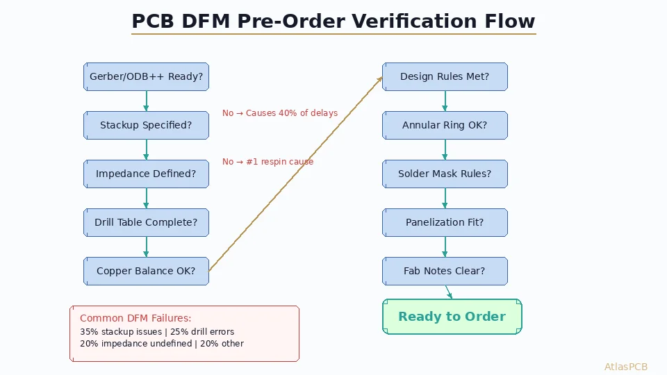
Before generating Gerber files, verify these items in your design:
- Run copper-to-copper DRC at your fabricator’s stated minimum (not your design intent minimum)
- Check annular ring on all vias: (Pad - Drill) / 2 >= 4mil
- Calculate aspect ratio: Board Thickness / Smallest Drill <= 10 (standard) or 16 (advanced)
- Verify drill-to-copper clearance >= 8mil on all non-connected features
- Check solder mask dam width on fine-pitch components (>= 3mil)
- Search for acid traps at trace junctions (no angles below 45 degrees)
- Verify copper balance: opposing layers within 15% fill area
- Confirm impedance targets are achievable with available prepreg thicknesses
- Check copper-to-edge clearance (10mil routed, 15mil V-score)
- Verify any via-in-pad is specified as filled/planarized
- Check minimum slot width is >= 0.8mm
- Verify silkscreen does not overlap exposed pads
Running this checklist takes 15-20 minutes and prevents an average of 2.3 days of DFM-related delay. It is the highest-ROI activity in the PCB design workflow.
ATLASPCB
Ready to Order? We Validate Your Design.
Every AtlasPCB order includes comprehensive DFM review by our process engineers. Catch issues before fabrication — not after shipping. Upload your Gerbers for a quote with DFM analysis.
Get Quote + DFM Review ›
Reviewed by AtlasPCB Engineering Team — 15+ years in advanced PCB fabrication for RF, HDI, and rigid-flex applications.
Related Reading:
About AtlasPCB — We specialize in complex PCB manufacturing for HDI, RF, and high-reliability applications. Explore our free engineering DFM review, or get an full PCB manufacturing capabilities . Every order includes free engineering review. Get your quote.
Reviewed by AtlasPCB Engineering Team — IPC-certified manufacturing specialists with 15+ years of production experience in HDI, RF, and high-reliability PCB fabrication. Content based on factory floor data and real customer design reviews.
Frequently Asked Questions
What is the most common PCB DFM failure?
How long does a DFM review take?
Should I run DFM check before or after layout is complete?
What PCB DFM checks do automated tools miss?
Does DFM review add to my PCB lead time?
- PCB DFM check
- design for manufacturability
- PCB fabrication
- DFM review
- PCB manufacturing