· David Okafor · Engineering · 11 min read
Rigid-Flex PCB DFM
Critical rigid-flex DFM rules that go beyond standard design rule checks. Covers transition zone violations, copper stress relief, coverlay overlap requirements, and bend zone plating — the issues that cause yield loss at the fabricator even when your design passes DRC.
Quick Answer
Standard EDA design rule checks validate trace width, spacing, and annular ring — but miss the seven rigid-flex-specific fabrication constraints that cause 60% of first-article rejections: transition zone via placement, copper thinning at flex entry, coverlay-to-rigid overlap, plated features in bend zones, adhesive squeeze-out margins, stiffener gap tolerances, and impedance discontinuity at material boundaries. These require manufacturer-specific process knowledge that changes with material system and buildup.
The Problem: DRC Green Does Not Mean Manufacturable
Every rigid-flex designer has experienced this frustration: the design passes all DRC checks in your EDA tool, you submit Gerber files to the manufacturer, and within 48 hours you receive a DFM report listing seven or eight issues that require design changes. The board is electrically correct and geometrically valid within the tool’s rule set — but it cannot be fabricated reliably with those specific geometry and material combinations.
This disconnect exists because rigid-flex fabrication is governed by process constraints that standard EDA design rules were never built to model. Your DRC validates copper geometry on flat layers. Rigid-flex manufacturing involves bending, sequential lamination across dissimilar materials, adhesive flow dynamics, and mechanical stress at material boundaries — none of which map to traditional 2D rule checks.
Based on our rigid-flex DFM review data from the past 18 months (approximately 800 designs reviewed), 62% of first-submission designs contain at least one of the following seven constraint violations. Most require straightforward modifications once identified — the issue is that they are not identified until the design reaches a fabricator with rigid-flex expertise.
Constraint 1: Via Placement Near Rigid-Flex Transitions
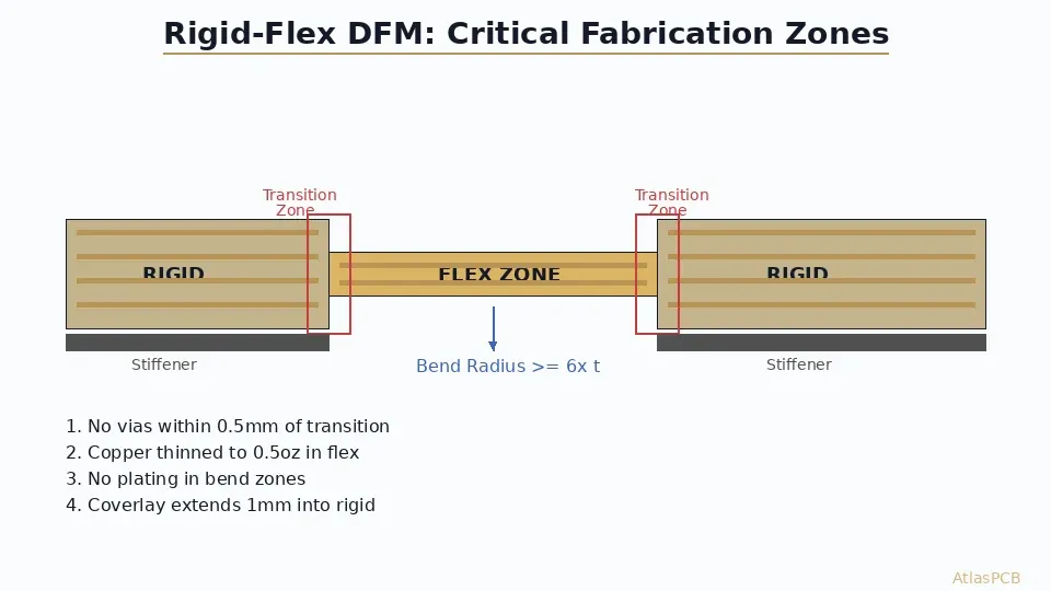
The most common violation we encounter — appearing in roughly 40% of submitted rigid-flex designs — is vias placed too close to the rigid-flex boundary line. Engineers naturally route traces through the transition zone and place vias wherever the BGA fanout or signal routing demands, without realizing that the transition zone imposes a hard keepout.
The physics are straightforward: during flex cycling, the rigid-flex boundary is the point of maximum stress concentration. The flex portion bends while the rigid portion remains stationary, creating a shear force at the interface. A plated via barrel is essentially a rigid cylinder embedded in the substrate — if it sits near this stress boundary, the barrel becomes a crack initiation site. We have cross-section data showing barrel cracks originating at exactly the transition boundary in boards where vias were placed within 0.3mm of the flex edge.
The manufacturing process compounds this issue. During sequential lamination, the rigid prepreg must flow and fill around features near the boundary. Vias close to the edge create resin-starved zones where the adhesive cannot fully encapsulate the pad-to-via connection, leading to delamination under thermal cycling.
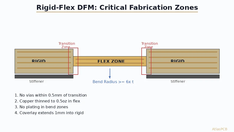
Rule: Keep all vias (including microvias) a minimum of 0.5mm from the rigid-flex boundary. For designs requiring IPC Class 3 reliability or flex cycle counts above 1,000, increase to 1.0mm minimum.
RIGID-FLEX EXPERTISE
Pre-Production DFM Review for Rigid-Flex Designs
Our process engineers review your rigid-flex design against 40+ fabrication constraints before quoting. Catch these issues before committing to tooling.
Submit Design for Review ›
Constraint 2: Copper Thinning at Flex Entry Points
When traces route from a rigid section into a flex zone, the copper transitions from being mechanically supported (embedded in rigid laminate) to being a free-standing conductor within the flexible polyimide. This transition creates a stress riser analogous to a notch in a fatigue specimen — if the copper cross-section remains constant, all bending strain concentrates at the exact point where rigid support ends.
The solution is copper tapering: gradually widening traces as they enter the flex zone so that the cross-sectional moment arm distributes stress over a longer distance. For standard 0.5oz RA copper in a dynamic flex application, we recommend widening traces by 50-100% over a 1-2mm taper length as they enter the bend zone. This simple geometry change extends flex fatigue life from thousands of cycles to hundreds of thousands.
The EDA tool issue: most tools model traces as constant-width features along their route. Implementing tapered entry points requires manual polygon adjustments or custom rules that few designers implement unless specifically guided by DFM feedback.
Rule: Taper trace width by 1.5x minimum over 1.0mm entry length at rigid-to-flex transitions. For dynamic flex (>100 cycles), use 2.0x taper over 2.0mm.
Constraint 3: Coverlay-to-Rigid Overlap
Coverlay is the polyimide film laminated over flex copper layers as the protective dielectric (analogous to solder mask on rigid sections). At the rigid-flex boundary, the coverlay must extend past the flex zone into the rigid section by a defined overlap distance. This overlap gets captured between the rigid laminate layers during pressing, anchoring the coverlay mechanically.
Insufficient overlap causes two failure modes. First, the coverlay edge can peel back during thermal cycling (solder reflow temperatures cause differential expansion between polyimide and FR-4). Second, moisture wicks along the interface between coverlay and rigid laminate if the seal is incomplete, leading to CAF (Conductive Anodic Filament) growth between adjacent conductors.
Rule: Coverlay overlap into rigid section: 1.0mm minimum, 1.5mm for high-reliability applications. Verify that your stackup drawing clearly dimensions this overlap — manufacturers cannot determine the correct overlap from Gerber data alone if the rigid-flex boundary definition is ambiguous.
Constraint 4: No Plated Features in Dynamic Bend Zones
This constraint seems obvious once stated, but violations appear in approximately 15% of submitted designs. Engineers occasionally route a trace through a bend zone and realize they need a layer transition — adding a via in the only available space, which happens to be in the flex bend area.
Any plated feature — through-hole via, blind via, or microvia — in a dynamic bend zone will fail. The plated copper barrel is rigid and cannot flex. Under repeated bending, the barrel cracks at the interface with the flex substrate, and the crack propagates until the connection opens. Typical cycles to failure: 10-50 for tight bend radii, 50-200 for gentle bends. This is not a “might fail” scenario — it is a guaranteed failure mechanism.
Static flex applications (fold once during assembly, never flex again) can tolerate plated features in the bend zone with appropriate derating, but our strong recommendation is to avoid them entirely. Route all layer transitions through vias placed in rigid sections, even if this requires longer trace paths.
Rule: Zero plated features permitted in dynamic bend zones. For static flex: no vias within 2mm of the bend centerline if the fold angle exceeds 90 degrees.
MANUFACTURING CAPABILITY
Rigid-Flex Up to 22 Layers
Sequential lamination with controlled impedance on flex layers. Polyimide, LCP, and adhesiveless constructions available.
Rigid-Flex Services ›Constraint 5: Adhesive Squeeze-Out Margins
Rigid-flex boards use adhesive layers (typically acrylic or epoxy-based) to bond the flex core to rigid buildup layers. During lamination under heat and pressure, this adhesive flows — and if copper features are too close to the rigid-flex boundary on the rigid side, adhesive squeeze-out can encroach onto pads or traces, causing resist adhesion failures or solder joint defects.
The squeeze-out distance depends on adhesive type, lamination parameters, and the volume of adhesive relative to the cavity it fills. In our process, typical squeeze-out ranges from 0.3mm to 0.8mm from the designed adhesive boundary. This means copper features on rigid layers near the transition must have at least 1.0mm clearance from the flex edge to avoid adhesive contamination.
This constraint is entirely invisible to EDA tools. The adhesive layer is typically not modeled as a design layer — it exists only in the fabrication stackup drawing. Designers who place components or route traces right up to the rigid-flex boundary on the rigid side will encounter this issue at DFM review.
Rule: No copper features within 1.0mm of the rigid-flex boundary on the rigid side (accounts for adhesive flow). No components within 2.0mm of the boundary.
Constraint 6: Stiffener Gap and Placement Tolerance
Stiffeners (FR-4 or polyimide reinforcement) are applied to flex areas that need temporary or permanent rigidity — typically under SMD component mounting areas on flex sections, or in ZIF connector zones. The gap between stiffener edge and the nearest bend zone is critical: too close, and the stiffener constrains the bend, creating a new stress concentration. Too far, and the component mounting area lacks adequate flatness for reliable solder joints.
Manufacturing tolerance on stiffener placement is typically ±0.2-0.3mm. This means your designed gap must account for worst-case placement error. If you design a 0.5mm gap between stiffener edge and bend start, manufacturing tolerance could reduce the actual gap to 0.2mm — creating a near-rigid constraint on the bend that dramatically increases copper stress.
Rule: Minimum designed gap between stiffener edge and bend zone start: 1.0mm. This provides adequate margin after manufacturing tolerance absorption and ensures the bend radius transition is smooth rather than abrupt.
Constraint 7: Impedance Discontinuity at Material Boundaries
The seventh constraint is electromagnetic rather than mechanical, but it causes functional failures rather than reliability failures. At the rigid-flex boundary, the transmission line environment changes: dielectric constant shifts from FR-4 (~4.2-4.5) to polyimide (~3.2-3.5), and the dielectric thickness often changes as the stackup transitions from a many-layer rigid construction to a thin flex core.
If impedance-controlled traces cross the rigid-flex boundary, there will be an impedance discontinuity unless the trace width is adjusted to compensate for the dielectric change. A 50-ohm trace on FR-4 with Dk=4.3 will become approximately 43-45 ohms when it enters polyimide with Dk=3.4 (for the same geometry), creating a reflection coefficient of 5-7%. For high-speed signals, this reflection degrades eye diagrams and can push a marginal link below specification.
The fix is trace width compensation at the boundary — narrowing the trace slightly as it enters the lower-Dk flex material. This requires the designer to perform impedance calculation for both material systems and implement a width transition at the boundary. Few EDA tools automate this for rigid-flex designs.
Rule: Calculate impedance separately for rigid and flex sections. Implement trace width compensation at boundaries for any signal operating above 2.5 Gbps. Provide both rigid and flex impedance targets to your manufacturer.
DFM BEFORE FABRICATION
Avoid Costly Rigid-Flex Respins
Our engineers review rigid-flex designs against all 7 constraints before production. Most issues resolved with minor modifications — saving weeks vs discovery at first article.
Upload Design ›Pre-Submission Checklist
Before sending your rigid-flex design to any manufacturer, verify these items that standard DRC cannot check:
- All vias are at least 0.5mm (preferably 1.0mm) from rigid-flex boundaries
- Traces taper to 1.5-2x width as they enter flex zones
- Coverlay overlap into rigid section is dimensioned at 1.0mm minimum
- No plated features exist in any dynamic bend zone
- No copper features within 1.0mm of the boundary on rigid layers
- Stiffener-to-bend gaps are 1.0mm minimum (accounting for ±0.3mm placement tolerance)
- Impedance-controlled traces have width compensation at material transitions
These seven constraints account for the majority of rigid-flex DFM rejections. Addressing them before submission eliminates the most common round-trip cycle between designer and fabricator, saving one to two weeks on your project timeline.
ATLASPCB
Rigid-Flex Design Ready for Fabrication?
Upload your design package for engineering review. We verify all transition zone constraints, material compatibility, and impedance continuity before generating tooling.
Get Rigid-Flex Quote ›
Reviewed by AtlasPCB Engineering Team — 15+ years in advanced PCB fabrication for RF, HDI, and rigid-flex applications.
Related Reading:
About AtlasPCB — We specialize in complex PCB manufacturing for HDI, RF, and high-reliability applications. Explore our rigid-flex PCB manufacturing, or get an free engineering DFM review . Every order includes free engineering review. Get your quote.
Reviewed by AtlasPCB Engineering Team — IPC-certified manufacturing specialists with 15+ years of production experience in HDI, RF, and high-reliability PCB fabrication. Content based on factory floor data and real customer design reviews.
Frequently Asked Questions
Why do rigid-flex designs fail DFM review even when they pass DRC?
How far from the rigid-flex transition should vias be kept?
What is the correct coverlay overlap into the rigid section?
Can I have plated through-holes in a flex bend zone?
What copper weight should be used in flex layers?
- rigid-flex PCB manufacturer
- PCB DFM check
- rigid-flex fabrication
- flex PCB design
- DFM guidelines