· David Okafor · Engineering · 9 min read
Multilayer PCB Cost
Detailed cost analysis of multilayer PCBs from 4 to 16 layers with actual pricing data. Understand the specific manufacturing steps that drive each cost jump, and learn which design decisions reduce per-board cost by 15-40% without sacrificing electrical performance.
Quick Answer
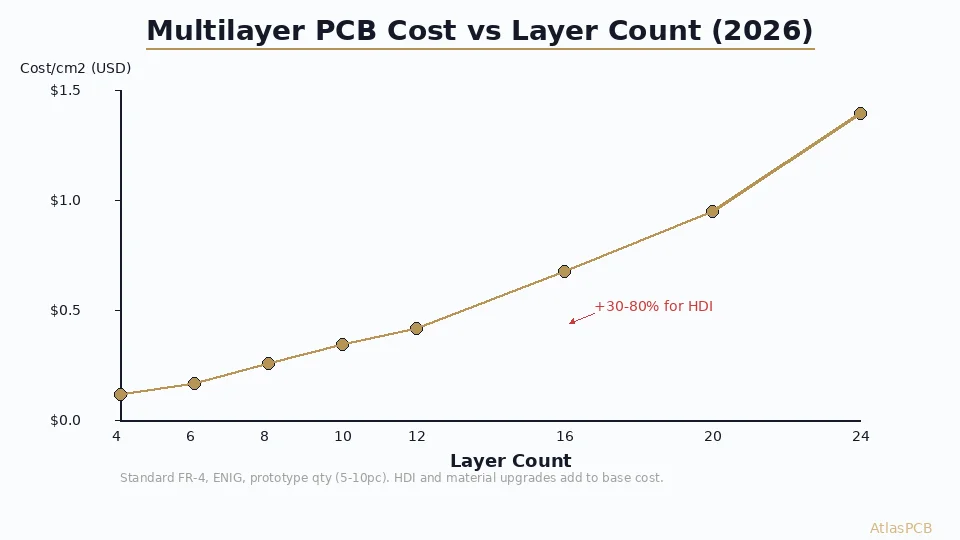
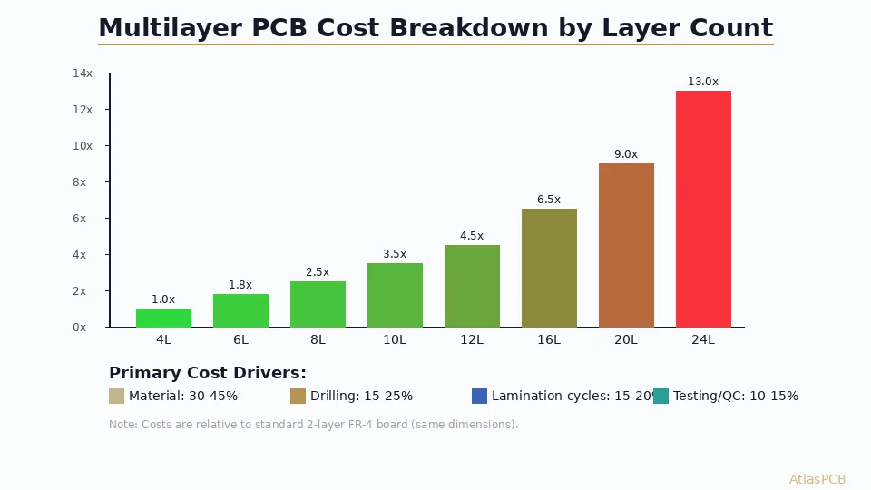
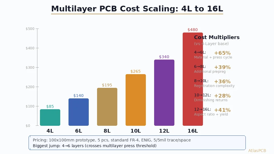
A 6-layer PCB costs approximately 65% more than a 4-layer of the same size due to a fundamental manufacturing threshold: crossing from single-press to sequential lamination. The cost jump from 6 to 8 layers (+39%) is smaller because the sequential press infrastructure already exists. Largest cost levers are via structure (through-hole vs blind/buried), minimum trace width (5mil costs 30% less than 3mil), and material grade. For production volumes above 500 pieces, optimizing panel utilization often saves more than reducing layer count.
Quick Cost Reference
Prototype pricing for 100x100mm boards, 5 pieces, standard FR-4, ENIG finish:
| Layer Count | Typical Cost | vs 4-Layer | Key Cost Driver |
|---|---|---|---|
| 4-Layer | $80-110 | Baseline | Single press cycle |
| 6-Layer | $130-180 | +65% | Sequential lamination threshold |
| 8-Layer | $180-250 | +125% | Additional lamination cycle |
| 10-Layer | $250-340 | +210% | Registration complexity |
| 12-Layer | $320-430 | +290% | Aspect ratio limits |
| 16-Layer | $450-600 | +450% | Yield drops, material cost |
These are actual prototype prices. Production quantities (1000+ pieces) reduce per-unit cost by 60-80% but maintain similar ratios between layer counts.
The Manufacturing Steps Behind Each Cost Jump
Understanding where money goes helps you identify which costs are compressible and which are fixed by physics.
4 to 6 Layers: The Sequential Lamination Threshold
A 4-layer board is manufactured in one press cycle: two copper-clad cores are bonded together with prepreg between them. All four layers are imaged and etched before the single lamination step. This is the simplest multilayer construction and benefits from maximum manufacturing efficiency.
Crossing to 6 layers introduces sequential processing. The inner 4-layer core is fabricated first (imaged, etched, laminated), then additional copper and prepreg layers are added and pressed in a second cycle. This second cycle requires re-alignment, re-drilling for registration targets, and exposes the inner layers to additional thermal stress.
From a cost perspective, the second lamination cycle nearly doubles processing time for the press equipment — the highest-cost bottleneck in PCB fabrication. Material cost increases only 30-40% (2 additional copper foils + prepreg), but process cost increases 80-100%. Combined, total board cost rises approximately 65%.
In our production line, the 4-layer to 6-layer transition also affects yield. Four-layer boards achieve 97-98% first-pass yield. Six-layer boards typically run 94-96% due to the additional registration tolerance stack-up and potential for inner-layer defects introduced during the second press cycle.
INSTANT PRICING
Get Exact Pricing for Your Layer Count
Upload your design files — our system generates pricing for 4, 6, 8, or 10-layer options with your exact specifications. Compare costs instantly and choose the best value.
Get Multi-Layer Quote ›
6 to 8 Layers: Incremental, Not Transformative
The 6-to-8 layer jump adds approximately 39% to cost — notably less than the 4-to-6 transition. The reason: the sequential lamination infrastructure (fixtures, alignment systems, multi-press scheduling) already exists for the 6-layer build. Adding two more layers means additional material cost and slightly longer press time, but no fundamental process change.
Material cost increases linearly: two more copper foils ($3-5 per panel) and one more prepreg sheet ($2-4). Process cost increases about 25%: longer imaging time for 2 additional layers, additional AOI inspection passes, and marginally longer drilling time for registration holes.
The yield impact is moderate — 8-layer boards typically achieve 92-95% first-pass yield compared to 94-96% for 6-layer. The slight yield reduction comes from cumulative registration tolerance and additional defect opportunity on inner layers.
8 to 12+ Layers: Diminishing Percentage Increases
Above 8 layers, cost increases per additional layer pair tend to decrease in percentage terms because fixed costs are increasingly amortized. The absolute dollar increase remains significant, but each additional pair becomes proportionally less expensive relative to the base cost.
However, new cost thresholds appear at higher layer counts:
10-12 layers: Aspect ratio begins to limit drill diameter. Standard 0.3mm drill in a 2.0mm thick board (6.7:1 aspect ratio) is fine. The same drill in a 2.8mm board (9.3:1) requires specialized drilling parameters and lower feed rates, adding 15-20% to drill time.
14-16 layers: Board thickness exceeds 2.5mm for standard copper weights, pushing into heavy-board processing territory. Panel flatness becomes critical, requiring post-lamination conditioning steps. Material cost increases non-linearly because thicker boards require more prepreg per layer to maintain dielectric targets.
20+ layers: Yield drops significantly (85-90% first-pass) due to cumulative registration error across 10+ imaging cycles. Every additional layer adds ±12-15μm of alignment uncertainty. At 20 layers, total registration uncertainty can exceed ±100μm — pushing annular ring limits and requiring design accommodation.
The Five Biggest Cost Levers (Ranked by Impact)
When optimizing multilayer PCB cost, these design parameters have the most impact — ranked by typical savings potential:
1. Via Structure (saves 20-40%)
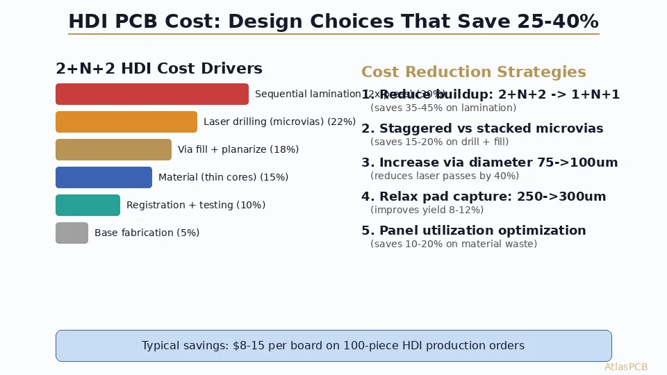
The single largest cost differentiation beyond layer count is via complexity. Through-hole vias are the cheapest — one mechanical drill operation creates a hole through all layers. Blind and buried vias require sequential processing: the inner via must be drilled, plated, and filled before outer layers are laminated. Each sequential drill-plate-fill cycle adds 20-30% to process cost.
If your 8-layer design uses blind vias on layers 1-2 and 7-8, but the design could alternatively route with through-hole vias and slightly wider trace spacing, the through-hole version saves 25-35% in fabrication cost. We regularly help engineers evaluate this tradeoff — whether the routing density gained by blind vias justifies their cost premium for a specific design.
2. Minimum Trace/Space (saves 15-30%)
Manufacturing yield is directly tied to feature size. At 5/5mil trace/space, our imaging and etching process achieves 98%+ yield on individual layers. At 4/4mil, yield drops to 95-96%. At 3/3mil, yield drops further to 92-94%. This yield difference compounds across multiple layers — an 8-layer board at 3/3mil has significantly higher scrap rate than the same board at 5/5mil.
The cost impact: 3/3mil designs require LDI (laser direct imaging) instead of standard photolithography, adding $10-20 per panel in equipment time. Combined with yield loss, a design at 3/3mil costs 30-50% more than the same design relaxed to 5/5mil. For many designs, routing at 5/5mil and adding one layer pair is cheaper than routing at 3/3mil.
3. Board Size and Panel Utilization (saves 15-25%)
A board dimension that wastes 30% of panel area costs 30% more per unit than a board that fills the panel efficiently. This sounds obvious, but we see it constantly — 105mm boards that waste an entire column if they were 100mm.
The standard manufacturing panel working area is approximately 400mm × 550mm (16” × 22”). Boards that fit the panel in clean arrays with minimal waste achieve lowest per-unit cost. The biggest panel utilization offenders are boards slightly over half-panel width: a 210mm board fits only once across the panel width, wasting 190mm of panel on the other side.
PANEL OPTIMIZATION
We Optimize Panel Layout for Every Order
Our quoting system calculates optimal panelization and suggests dimension adjustments that can reduce per-unit cost by 15-25% — especially impactful at production volumes.
Get Cost-Optimized Quote ›4. Material Grade (saves 10-20%)
Standard FR-4 (Tg 135-150°C) is the cheapest base material. Moving to mid-Tg (170°C) adds 8-12% to material cost. High-Tg (180°C+) adds 15-20%. Low-loss materials (Megtron 4/6, IT-968) add 40-100%.
The optimization question: does your design actually need high-Tg material? If your assembly uses lead-free solder with peak reflow at 245°C, standard Tg 150 material may not have sufficient margin. But if you are using SnAgCu solder with controlled reflow at 235°C peak, standard material often suffices with proper thermal profile management.
For high-speed designs, the material cost tradeoff is between using expensive low-loss material at lower layer count versus cheaper FR-4 at higher layer count with shorter trace runs. A 6-layer board on Megtron 6 may deliver equivalent signal performance to an 8-layer board on standard FR-4 — but the cost comparison depends on your specific volume and trace lengths.
5. Surface Finish (saves 5-15%)
HASL (hot air solder leveling) is the cheapest surface finish but creates uneven pad surfaces unsuitable for fine-pitch components. ENIG is the most common mid-range option (adds $10-25 per panel). OSP is cheaper than ENIG but has shelf-life limitations.
For cost-optimized production: use OSP if boards will be assembled within 3 months of fabrication and do not require wire bonding or edge connectors. Use ENIG for longer shelf life, consistent flat pads, and wire bonding compatibility. Reserve Immersion Silver or ENEPIG for specific requirements (silver: lowest cost flat finish; ENEPIG: wire bonding + soldering on same board).
Real-World Optimization Examples
Case: Network Switch (10G) — Reduced from $340 to $210 per board
Original specification: 12-layer, 3/3mil, blind/buried vias, Megtron 6, ENIG. Our DFM review found that only 2 signal layers actually carried 10G traces — the rest were 1G SGMII and management interfaces that could tolerate standard FR-4.
Optimized: 10-layer hybrid (Megtron 6 on layers 1/2 and 9/10, standard FR-4 inner), relaxed to 4/4mil on non-critical layers, eliminated blind vias by rerouting through standard through-holes with backdrilling. Result: 38% cost reduction with equivalent signal integrity on 10G channels.
Case: IoT Sensor Module — Avoided unnecessary layer upgrade
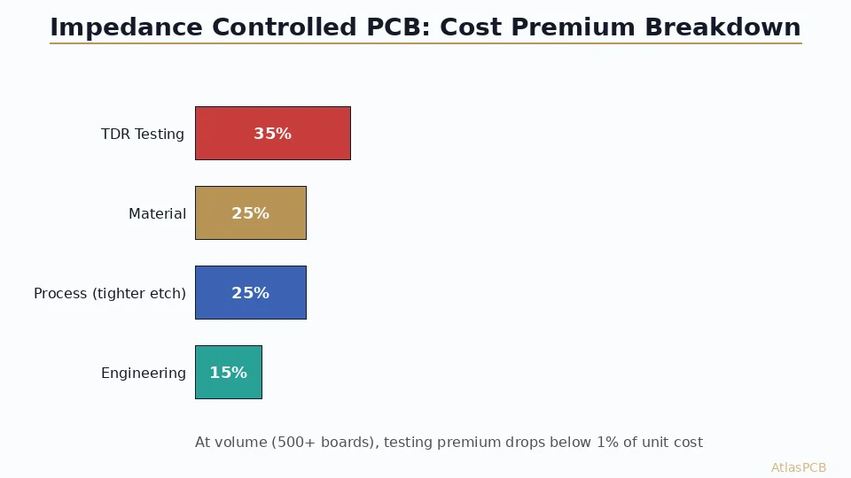
Engineer requested 6-layer board for an nRF52 BLE design. Our stackup review showed: the design only used 23% of Layer 3 routing capacity, and the 2.4 GHz antenna trace was the only impedance-critical element. By optimizing the 4-layer stackup (placing ground pour beneath antenna trace, using 3.5mil prepreg for that specific dielectric height), we achieved the required 50-ohm antenna impedance on a 4-layer board — saving 40% versus the 6-layer quote.
ATLASPCB
Multilayer PCB — From 4 to 30 Layers, Cost-Optimized
Upload your design for instant pricing across layer count options. Our engineering team identifies cost optimization opportunities — often saving 20-30% without performance compromise.
Get Multilayer Quote ›
Reviewed by AtlasPCB Engineering Team — 15+ years in advanced PCB fabrication for RF, HDI, and rigid-flex applications.
Related Reading:
About AtlasPCB — We specialize in complex PCB manufacturing for HDI, RF, and high-reliability applications. Explore our HDI PCB manufacturing capabilities, multilayer PCB fabrication up to 30 layers, or get an instant online PCB quote . Every order includes free engineering review. Get your quote.
Reviewed by AtlasPCB Engineering Team — IPC-certified manufacturing specialists with 15+ years of production experience in HDI, RF, and high-reliability PCB fabrication. Content based on factory floor data and real customer design reviews.
Frequently Asked Questions
Why does a 6-layer PCB cost so much more than a 4-layer?
How much does each additional layer pair add to PCB cost?
What is the cheapest way to add more routing layers?
Does minimum trace width significantly affect PCB cost?
When is HDI cheaper than adding more standard layers?
- multilayer PCB cost
- PCB pricing
- PCB stackup design guide
- HDI PCB manufacturer
- PCB manufacturing