· David Okafor · Engineering · 6 min read
HDI PCB Cost Breakdown
Understand exactly what makes HDI PCBs expensive and where you can save money without sacrificing performance. Real pricing data for 1+N+1 through 5+N+5 buildups with cost optimization strategies.
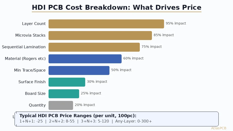
Quick Answer
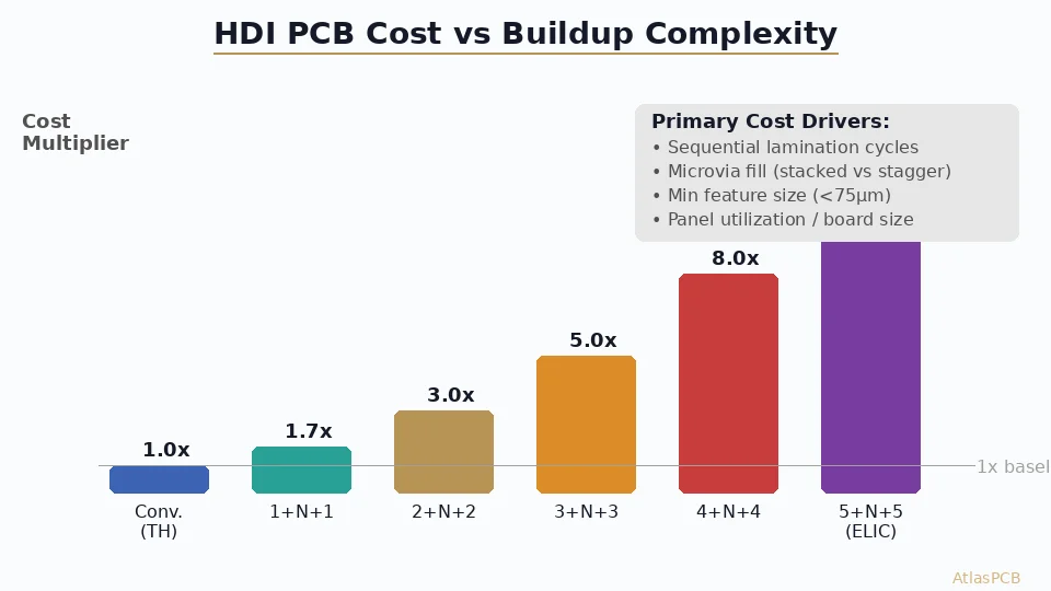
HDI PCB costs are driven primarily by sequential lamination cycles (each adds 30-50% to base cost), microvia stacking depth (stacked microvias cost 2-3x staggered), and minimum trace/space requirements (below 3/3mil requires semi-additive process at 4-8x cost). A typical 8-layer 1+N+1 HDI board costs $15-35/unit at 100pc quantity; a 12-layer 2+N+2 costs $30-70; and a 16-layer 3+N+3 costs $60-150. Optimization strategies include reducing via stack depth, using staggered instead of stacked microvias, and keeping trace/space at 3/3mil or above.
HDI Pricing at a Glance
| HDI Structure | Layer Count | Price Range (100pc, 50x50mm) | Key Cost Driver |
|---|---|---|---|
| 1+N+1 | 6-8L | $12-35/unit | 1 laser drill + 1 extra press |
| 2+N+2 (staggered) | 8-12L | $25-60/unit | 2 sequential laminations |
| 2+N+2 (stacked) | 8-12L | $35-80/unit | Via fill + cap between cycles |
| 3+N+3 | 12-16L | $55-150/unit | 3 sequential laminations |
| 4+N+4 | 16-20L | $90-220/unit | Process complexity, yield loss |
| 5+N+5 / ELIC | 16-24L | $120-300+/unit | Maximum process complexity |
These prices assume: FR-4 Tg170, ENIG finish, 3/3mil trace/space, standard panel size. Prices increase with board area, special materials, and tighter tolerances.
The 5 Major Cost Drivers (Ranked by Impact)
1. Sequential Lamination Cycles (+30-50% per cycle)
Every “+N+” in the HDI buildup means another complete lamination cycle. Each cycle includes:
- Laser drilling of microvias
- Desmear and plating
- Imaging and etching
- Lamination press (4-6 hour cycle)
- Alignment verification
A standard 8-layer board goes through the press once. A 1+N+1 goes through twice. A 3+N+3 goes through four times. Each additional press cycle adds 30-50% to the base fabrication cost because it’s essentially building another board on top of your board.
2. Microvia Configuration (+50-200%)
| Via Type | Cost Impact | When Required |
|---|---|---|
| Single-depth microvia | Baseline HDI | 0.65mm+ pitch BGA |
| Staggered multi-depth | +30-50% | 0.5mm pitch BGA |
| Stacked (filled+capped) | +80-150% | 0.4mm pitch BGA |
| Stacked 3+ deep | +150-200% | 0.3mm pitch / any-layer |
| Via-in-pad (VIPPO) | +20-40% | Fine-pitch BGA, RF |
Stacked microvias require copper-filling each via and planarizing before the next buildup layer—an extra plating and polishing step per stack depth.
3. Minimum Trace and Space
| Trace/Space | Process | Cost Multiplier |
|---|---|---|
| 4/4mil (100um) | Standard subtractive | 1x (baseline) |
| 3.5/3.5mil (90um) | Fine-line subtractive | 1.2-1.5x |
| 3/3mil (75um) | Advanced subtractive | 1.5-2x |
| 2/2mil (50um) | Modified semi-additive (mSAP) | 4-6x |
| 1.5/1.5mil (40um) | Semi-additive process | 6-10x |
Going below 3/3mil trace/space is where costs jump dramatically. If your BGA fanout works at 3/3mil, stay there.
HDI EXPERTISE
Get an Accurate HDI Quote in 24 Hours
Upload your design files. We'll identify the optimal HDI structure and provide detailed cost breakdown by line item.
Compare Prices ›
4. Material Selection (+0-300%)
Standard FR-4 Tg170 is the baseline for HDI. Premium materials add significantly:
| Material | Use Case | Premium vs FR-4 |
|---|---|---|
| FR-4 Tg170 | Standard HDI | Baseline |
| Megtron 4 (Mid-loss) | 10-16 Gbps signals | +40-60% |
| Megtron 6 (Low-loss) | 25-56 Gbps signals | +80-120% |
| Megtron 7 (Ultra-low) | 112 Gbps PAM4 | +150-200% |
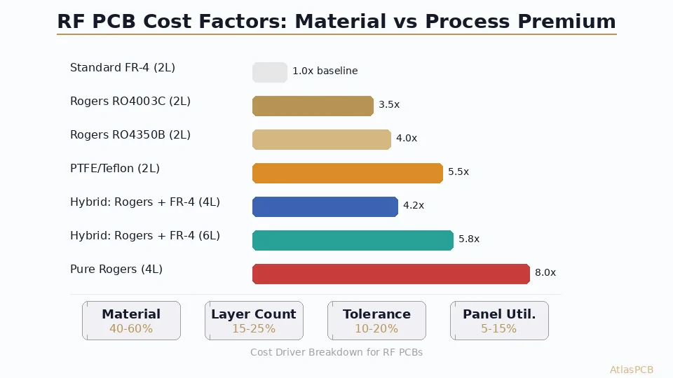
| Rogers + FR-4 hybrid | RF + digital combo | +100-300% |
For most HDI applications below 10 Gbps signal rates, standard FR-4 Tg170 or Tg180 is perfectly adequate. Save the premium laminates for boards that genuinely need them.
5. Quantity and Panel Utilization
HDI has high non-recurring engineering (NRE) cost due to laser drill programming, multi-stage alignment fixtures, and impedance modeling. This NRE gets amortized across quantity:
| Quantity | Typical Unit Cost (8L 1+N+1) | Cost per Extra Unit |
|---|---|---|
| 5 pieces | $50-80 | $45-70 |
| 20 pieces | $28-45 | $20-35 |
| 100 pieces | $15-28 | $12-22 |
| 500 pieces | $10-18 | $8-14 |
| 2000+ pieces | $7-14 | $5-10 |
Panel utilization also matters. A 50x50mm board fits 24-up on a standard 18x24” panel. A 100x80mm board fits only 6-up—quadrupling the per-unit panel cost.
8 Strategies to Reduce HDI Cost
1. Question Whether You Actually Need HDI
The most expensive HDI board is one you didn’t need. Before committing to HDI:
- Can you escape your BGA with blind+buried vias instead of microvias?
- Would 2 extra standard layers be cheaper than HDI?
- Can you upsize the BGA to 0.8mm pitch (eliminating HDI need)?
2. Use 1+N+1 Instead of 2+N+2
If you can escape all BGAs through a single microvia layer (even with some through-vias), stay at 1+N+1. The jump from 1+N+1 to 2+N+2 adds 40-60% cost.
3. Staggered Over Stacked
Unless you have 0.4mm pitch BGAs, staggered microvias typically provide sufficient routing density at 60-70% the cost of stacked.
4. Maximize Through-Via Usage
Only use microvias where you absolutely need them (under BGAs). Everything else can be standard through-hole or blind vias drilled mechanically.
5. Keep Trace/Space at 3/3mil or Above
The cost cliff below 3/3mil is steep. Design your BGA fanout to work at 3/3mil—often possible with proper via placement strategy.
6. Optimize Board Size for Panel Yield
Adjust board outline by 1-2mm to fit more boards per panel. Ask your fabricator for their panel size and optimal board dimensions.
7. Consolidate Orders
If you order HDI prototypes monthly, consolidating into bi-monthly orders of larger quantity can save 20-30% per unit.
8. Accept Longer Lead Time
Rush HDI (5-7 day) costs 50-100% more than standard (15-18 day). Plan ahead.
COST OPTIMIZATION
HDI Design Review: Reduce Cost Without Sacrificing Performance
We analyze your HDI stackup for cost-saving opportunities—stacked-to-staggered conversion, layer count reduction, trace width optimization.
Get Cost Analysis ›Real-World Pricing Examples
Example 1: Smartphone Application Processor Board
- 10-layer 2+N+2 (stacked microvias)
- 0.4mm pitch BGA, 3/3mil trace/space
- 40x40mm, FR-4 Tg170, ENIG
- 100pc: $38-52/unit | 1000pc: $18-28/unit
Example 2: 5G Baseband Processing Board
- 14-layer 3+N+3 (staggered)
- 0.5mm pitch BGA, 3.5/3.5mil trace/space
- 120x80mm, Megtron 4, ENIG
- 20pc: $95-140/unit | 200pc: $55-85/unit
Example 3: AI Accelerator Carrier
- 20-layer 4+N+4 (stacked, VIPPO)
- 0.4mm pitch, 3/3mil trace/space
- 200x150mm, Megtron 6, ENIG
- 10pc: $280-400/unit | 100pc: $150-220/unit
HDI CAPABILITIES
Up to 5+N+5 HDI with Stacked Microvias
Laser drill 0.075mm, via-in-pad, 3/3mil trace/space. From prototype to production quantities.
View HDI Capabilities ›When HDI Saves Money (Despite Higher Per-Board Cost)
HDI isn’t always the expensive option. Consider total system cost:
- Layer reduction: 12-layer standard → 8-layer HDI saves 2-4 layers
- Board size reduction: Denser routing → smaller board → smaller enclosure
- Fewer boards: Higher integration → fewer boards in the system
- Better signal integrity: Shorter vias → fewer termination resistors → lower BOM cost
- Higher yield in assembly: Better pad access → fewer solder defects
For a high-density design, the HDI premium may be offset by these system-level savings.
ATLASPCB
Get Your HDI Quote with Full Cost Breakdown
We itemize every cost factor so you can make informed optimization decisions. Upload your Gerber files for a detailed quote.
Get Instant Quote ›
Related Reading:
About AtlasPCB — We specialize in complex PCB manufacturing for HDI, RF, and high-reliability applications. Explore our HDI PCB manufacturing capabilities, PCB prototype manufacturing from 1 piece, or get an instant online PCB quote . Every order includes free engineering review. Get your quote.
Reviewed by AtlasPCB Engineering Team — IPC-certified manufacturing specialists with 15+ years of production experience in HDI, RF, and high-reliability PCB fabrication. Content based on factory floor data and real customer design reviews.
Frequently Asked Questions
How much more does HDI cost compared to standard multilayer PCB?
What's the cost difference between stacked and staggered microvias?
At what point does ELIC (Every Layer Interconnect) become cost-effective?
How can I reduce HDI PCB cost without changing my design?
- HDI PCB
- PCB cost
- pricing
- microvia
- sequential lamination
- via-in-pad
- PCB prototype