· Sophia Reyes · Engineering · 4 min read
How Many Layers Does My PCB Need? A Decision
Practical decision framework for PCB layer count selection. Covers signal density analysis, power distribution requirements, impedance control needs, and cost implications from 2-layer to 30+ layer designs.
Quick Answer
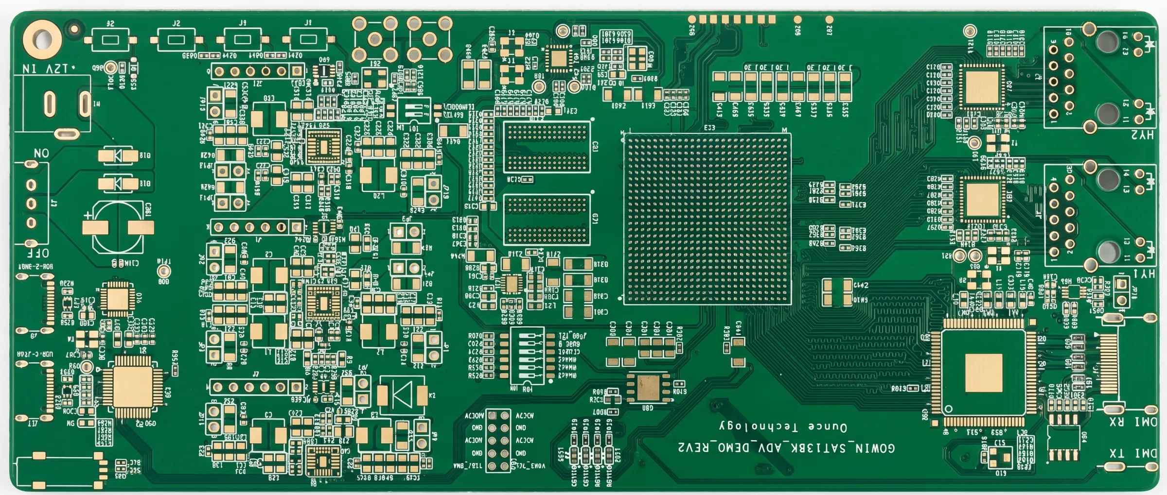
PCB layer count is determined by four factors: component density and routing channels required, power distribution complexity (number of voltage rails), controlled impedance requirements (each impedance-controlled signal layer needs an adjacent reference plane), and EMI/EMC compliance needs. A general guideline: 2 layers for simple designs under 50 components, 4 layers when impedance control or ground planes are needed, 6–8 layers for moderate-complexity digital designs with BGAs, 10–16 layers for high-speed digital with multiple SerDes interfaces, and 16–30+ layers for networking, server, and telecom equipment.
How Many Layers Does My PCB Need? A Decision Framework
Choosing the right layer count is one of the most impactful early decisions in PCB design. Too few layers forces compromises—routing congestion, impedance control violations, and EMI failures. Too many layers wastes money on manufacturing overhead that delivers no benefit.
This guide provides a systematic framework for determining the optimal layer count based on your design’s actual requirements.
The Four Factors That Drive Layer Count
Factor 1: Routing Density
The most intuitive factor—can you physically route all connections on the available signal layers?
Estimation method: Count the total number of signal nets, estimate the average route length, and calculate whether the available routing area accommodates all traces with required spacing.
Quick rules of thumb:
- 2 layers: Up to 50 components, single-sided placement preferred
- 4 layers: Up to 200 components, moderate density BGAs (0.8mm+ pitch)
- 6–8 layers: Up to 500 components, fine-pitch BGAs (0.5–0.65mm pitch)
- 10–16 layers: High-pin-count FPGAs, multiple processors, high-speed connectors
- 16–30+: Server/networking boards with dense BGA fields and hundreds of differential pairs
Factor 2: Power Distribution
Each distinct power rail ideally gets a dedicated copper plane or wide routing channel:
| Power Complexity | Typical Layers for Power | Total Board Layers |
|---|---|---|
| Single 3.3V + GND | 1 power + 1 ground plane | 4+ |
| 3.3V + 1.8V + GND | 1 split power + 1 ground | 4–6 |
| Core + I/O + analog + GND | 2 power + 2 ground | 8+ |
| Multiple cores + SerDes + DDR + analog | 3+ power + 3+ ground | 12+ |
Factor 3: Impedance Control Requirements
Controlled impedance requires that every signal layer have an adjacent reference plane (ground or power). This is the factor that most commonly forces additional layers:
- No impedance control: 2 layers may suffice
- Single-ended 50Ω on 1–2 layers: 4 layers minimum (signal + ground reference)
- Differential pairs on 4+ layers: 8–10 layers minimum
- Full impedance control on all signal layers: Layer count = 2× signal layers (each signal layer needs a reference plane)
Factor 4: EMI/EMC Compliance
A continuous ground plane adjacent to signal traces is the single most effective EMI mitigation technique:
- Without ground plane: Radiated emissions often exceed FCC/CE limits by 10–20 dB
- With ground plane (4+ layers): Immediate 20–30 dB reduction in radiated emissions
- With ground plane on both sides of signal layer (stripline): Additional 10–15 dB suppression
Layer Count by Application
| Application | Typical Layer Count | Key Driver |
|---|---|---|
| Simple sensors, LED lighting | 2 | Cost |
| IoT devices, Bluetooth/WiFi | 4 | Ground plane for antenna |
| Consumer electronics, tablets | 4–6 | Routing density |
| Industrial controls, motor drives | 4–6 | Power distribution |
| Embedded computing, SBCs | 6–8 | BGA breakout |
| Telecom line cards | 8–12 | High-speed routing |
| GPU/CPU motherboards | 8–12 | Power + high-speed |
| Server mainboards | 12–20 | Complex power + DDR5 |
| Network switches | 16–32 | SerDes density |
| Backplanes | 20–40 | Connector density |
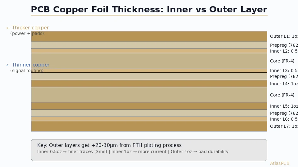
See our [multilayer PCB stackup design guide]/blog/multilayer-pcb-stackup-design-guide/) for detailed stackup configurations.
Cost Impact of Layer Count
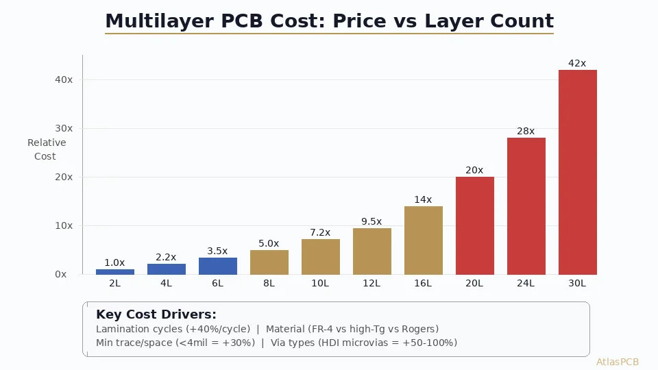
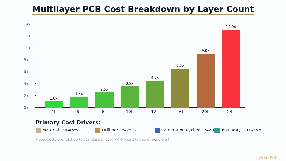
| Layers | Relative Cost | Primary Cost Driver |
|---|---|---|
| 2 | 1.0× | Baseline |
| 4 | 1.8–2.2× | Additional lamination + drilling |
| 6 | 2.5–3.0× | Third lamination cycle |
| 8 | 3.0–3.5× | Material + registration |
| 10 | 3.5–4.5× | Sequential lamination may start |
| 12 | 4.5–5.5× | Registration complexity |
| 16 | 6.0–8.0× | Material + registration + yield |
| 20+ | 8.0–15.0× | Specialized manufacturing |
Cost optimization tip: An 8-layer board on 3/3 mil trace/space is often cheaper than a 6-layer board requiring 2/2 mil rules. The additional layers cost less than the yield loss from tighter design rules. Use our [PCB stackup calculator]/blog/pcb-stackup-calculator/) to explore alternatives.
When to Add vs. Remove Layers
Signs You Need More Layers
- Autorouter completion rate below 85%
- Forced to route high-speed signals on layers without ground reference
- Unable to maintain 3W spacing between critical signal groups
- Power integrity simulations show excessive voltage drop
- EMC pre-compliance testing fails radiated emissions
Signs You Have Too Many Layers
- Signal layers with less than 40% utilization
- Power planes with only 1–2 narrow traces
- No impedance-controlled signals on inner layers
- Board thickness exceeding mechanical constraints
Ready to finalize your layer count? Upload your design for a free stackup optimization review.
Further Reading
- [Multilayer PCB Stackup Design Guide]/blog/multilayer-pcb-stackup-design-guide/)
- [PCB Stackup Calculator]/blog/pcb-stackup-calculator/)
- [Single Layer vs Multi Layer PCB]/blog/single-layer-vs-multi-layer-pcb/)
About AtlasPCB — We specialize in complex PCB manufacturing for HDI, RF, and high-reliability applications. Explore our multilayer PCB fabrication up to 30 layers . Every order includes free engineering review. Get your quote.
Reviewed by AtlasPCB Engineering Team — IPC-certified manufacturing specialists with 15+ years of production experience in HDI, RF, and high-reliability PCB fabrication. Content based on factory floor data and real customer design reviews.
Frequently Asked Questions
When do I need more than 4 PCB layers?
Does adding more PCB layers always increase cost?
What is the most common PCB layer count for IoT devices?
- pcb-design
- stackup-design
- layer-count
- cost-optimization