· David Okafor · Engineering · 7 min read
HDI PCB Manufacturer Pricing: Cost 1n1
Detailed cost analysis comparing 1+N+1 and 2+N+2 HDI build-ups. Understand why each additional microvia layer adds 35-50% to PCB cost, which design choices drive the premium, and when 2+N+2 delivers enough routing density to avoid adding expensive standard layers.
Quick Answer
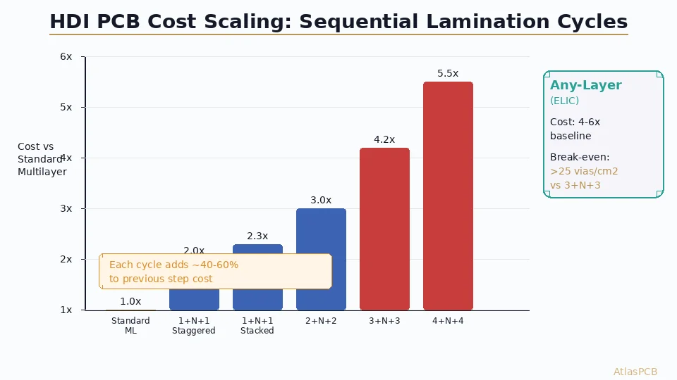
A 1+N+1 HDI build-up (microvias on outer layers only) adds 30-45% cost over an equivalent-layer standard through-hole PCB. Stepping to 2+N+2 (two sequential microvia layers per side) adds another 35-50% on top of 1+N+1 due to the additional sequential lamination cycle, laser drilling pass, and imaging step. The key decision: if your BGA pitch is 0.65mm or above, 1+N+1 usually provides sufficient breakout; below 0.5mm pitch, 2+N+2 or any-layer becomes necessary regardless of cost.
Quick Cost Reference: HDI Build-Up Pricing
Prototype pricing for 100x100mm boards, 10 pieces, standard FR-4, ENIG finish:
| Configuration | Layer Count | Typical Cost | vs Standard Equiv. | Key Cost Driver |
|---|---|---|---|---|
| Standard 8L | 8 | $180-250 | Baseline | Through-hole only |
| 1+6+1 HDI | 8 | $250-360 | +35-45% | 1 laser drill pass + 1 sequential lam |
| 2+4+2 HDI | 8 | $380-520 | +110-115% | 2 laser drill passes + 2 sequential lam |
| Standard 10L | 10 | $250-340 | Baseline-10L | Additional through-hole layer pair |
| 1+8+1 HDI | 10 | $330-450 | +30-35% vs 10L std | 1 laser drill + 1 sequential lam |
| 2+6+2 HDI | 10 | $480-650 | +90-95% vs 10L std | 2 laser drill + 2 sequential lam |
| 3+4+3 (Any-layer) | 10 | $700-950 | +180% vs 10L std | 3 laser cycles, via fill each stage |
The cost escalation is driven by one core fact: each additional microvia layer requires a full lamination cycle — which means the board goes through press, imaging, drilling, plating, and inspection an additional time. The board literally gets “built” three separate times in a 2+N+2 process.
Understanding the Cost Structure: Where the Money Goes
HDI cost breaks down into clearly identifiable process steps, each adding measurable cost:
1+N+1 Cost Breakdown (vs Standard)
| Process Addition | Cost per Panel | % of Premium |
|---|---|---|
| Laser drilling (CO₂/UV) | $40-80 | 35-40% |
| Sequential lamination | $20-40 | 18-22% |
| Additional imaging (microvia layer) | $15-25 | 12-15% |
| Microvia plating | $15-25 | 12-15% |
| Additional inspection/AOI | $10-20 | 8-12% |
| Via fill + planarization (if VIP) | $30-60 | 20-30%* |
*Via-in-pad adds this cost only when required for BGA escape
Why 2+N+2 Costs More Than Double 1+N+1’s Premium
The step from 1+N+1 to 2+N+2 is not simply “twice the laser drilling.” It requires:
- First microvia layer must be filled and planarized before the second layer is built on top — adding a copper fill step ($30-60)
- Registration tolerance accumulates — the second sequential lam must align to the already-processed first layer, requiring tighter equipment calibration and increasing scrap rate
- Total board time in production effectively doubles — a 2+N+2 board spends 5-7 days in process versus 3-4 days for 1+N+1, tying up equipment and queue slots
These factors explain why 2+N+2 costs 35-50% more than 1+N+1, not 100% more: the base infrastructure (inner core, outer processing) is shared.
HDI PCB MANUFACTURER
1+N+1 Through Any-Layer HDI — Competitive Pricing
From simple microvia breakout to 5+N+5 any-layer builds. Upload your design for a detailed quote with build-up options and DFM review.

When HDI Saves Money: The Layer Reduction Argument
The counterintuitive economics of HDI: a more expensive process can produce a cheaper board when the routing density gain eliminates layers.
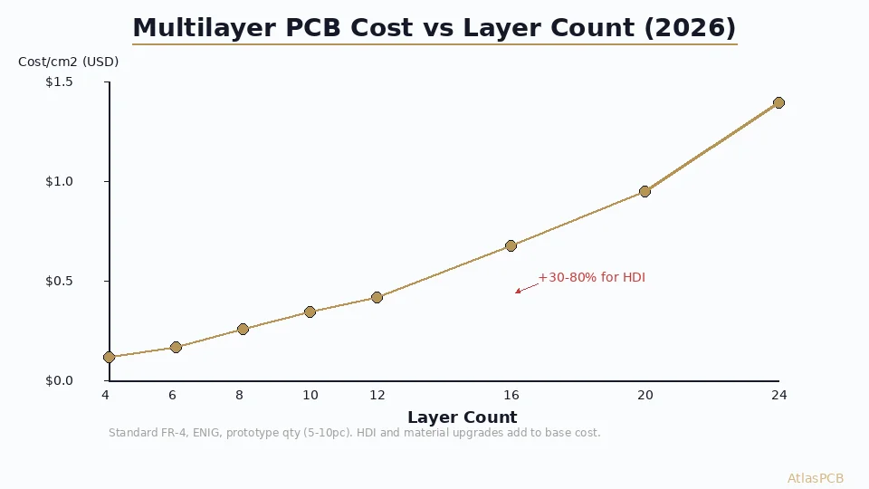
Consider a design requiring 45,000 routing connections in 60x60mm (typical high-pin-count FPGA or SoC board). Standard through-hole construction at 4/4mil trace/space requires approximately 12-14 layers to route successfully. HDI with 1+N+1 can achieve the same routing in 10 layers (1+8+1). With 2+N+2, it might fit in 8 layers (2+4+2).
| Approach | Layers | Estimated Cost (10pc prototype) | Production (1000pc) |
|---|---|---|---|
| Standard 14L | 14 | $450-600 | $18-25/ea |
| Standard 12L | 12 | $350-470 | $14-19/ea |
| 1+8+1 HDI | 10 | $330-450 | $12-16/ea |
| 2+4+2 HDI | 8 | $380-520 | $10-14/ea |
At prototype quantities, 1+8+1 HDI is already cheaper than the standard 14-layer it replaces. At production volumes, 2+4+2 HDI becomes the cheapest option despite using the most advanced process — because material and basic lamination costs scale with layer count while HDI process costs are relatively fixed per panel.
This is the key insight: HDI is expensive per step, but each step replaces TWO standard layers. When standard layer count would exceed 12, calculate whether HDI reduces enough layers to offset its process premium.
BGA Pitch and Build-Up Selection
The component driving your HDI decision is almost always a fine-pitch BGA. The escape routing from BGA pads determines minimum build-up:
| BGA Pitch | Rows Escapable per Layer | Minimum Build-Up | Notes |
|---|---|---|---|
| 1.0mm | 3-4 rows | Standard (dog-bone) | Through-hole vias between pads |
| 0.8mm | 2-3 rows | Standard or 1+N+1 | Via-in-pad recommended |
| 0.65mm | 1-2 rows | 1+N+1 minimum | Via-in-pad required |
| 0.5mm | 1 row | 1+N+1 or 2+N+2 | Depends on total pin count |
| 0.4mm | 0-1 row | 2+N+2 minimum | Any-layer for >400 pins |
| 0.3mm | 0 rows | 3+N+3 or any-layer | All escape through microvias |
For a 900-pin BGA at 0.8mm pitch, the outer 3-4 rows (approximately 120 pins) escape on the top layer. The next 2-3 rows escape through L1 microvias to L2 routing. With 1+N+1, you get one additional escape layer — usually sufficient for the inner pin field. If the BGA has more than 600-700 signal pins, the single escape layer becomes congested and 2+N+2 provides relief.
BGA ESCAPE ANALYSIS
Not Sure Which HDI Build-Up You Need?
Upload your BGA footprint and placement — our engineers determine minimum build-up requirements and provide cost comparison across 1+N+1, 2+N+2, and any-layer options.
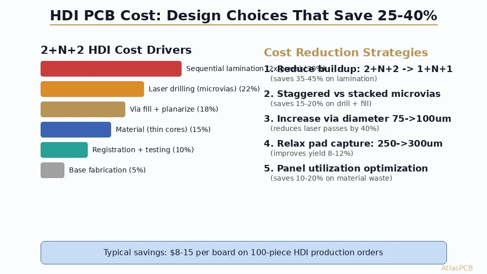
Get Build-Up Recommendation ›Design-for-Cost Strategies: Reducing HDI Premium by 15-30%
Several design decisions directly affect HDI cost without sacrificing functionality:
1. Microvia Pad Size Optimization
Standard microvia pad is 350μm with 150μm laser drill. If your design can use 300μm pads with 100μm drill (our minimum capability), the tighter geometry allows routing traces between via pads — potentially eliminating one routing layer. Each eliminated layer saves 10-15% of total board cost.
2. Staggered vs Stacked Microvia Selection
If your 2+N+2 design does not require connections from L1 directly to L3 (spanning two microvia layers), use staggered vias. This eliminates the copper fill and planarization step between sequential layers — saving $30-60 per panel or approximately 8-12% of total cost.
3. Via-in-Pad Only Where Necessary
Via-in-pad (VIP) requires filling and planarizing microvias to create a flat surface for BGA soldering. This adds $30-60 per panel. For areas of the board without BGA components, use standard dog-bone escape with the microvia offset from the pad — same routing benefit without the fill cost.
4. Panel Utilization Optimization
HDI processing costs are per-panel, not per-board. A 18x24 inch panel costs the same to process whether it contains 4 boards or 16. Optimizing board outline for maximum panelization directly reduces per-unit cost. For small boards (<50x50mm), HDI cost per unit can drop 40-60% by fitting 16+ boards per panel versus the 4-6 that large boards achieve.
5. Material Selection for HDI Layers
Standard FR-4 works for most HDI builds. However, if your microvia layers also require controlled impedance, specifying mid-Dk materials (Megtron 4/6) on HDI layers adds 20-30% material premium. If impedance control is only needed on inner standard layers, you can use generic FR-4 for the microvia buildup and save the material premium.
Volume Economics: HDI Cost Scaling
The per-unit cost curve for HDI flattens faster than standard PCBs because the dominant cost drivers (laser drilling, sequential lamination) are panel-level fixed costs:
| Quantity | 1+8+1 HDI per Unit | Standard 10L per Unit | Premium % |
|---|---|---|---|
| 5 pc | $33-45 | $25-34 | 35-45% |
| 50 pc | $15-22 | $11-16 | 32-40% |
| 500 pc | $9-13 | $7-10 | 25-35% |
| 5,000 pc | $6-9 | $5-7 | 20-28% |
| 50,000 pc | $4.5-6.5 | $4-5.5 | 15-20% |
At 50,000 pieces, HDI adds only $0.50-1.50 per board over standard — often less than the cost difference of one additional standard layer pair. This is why every smartphone in your pocket uses any-layer HDI despite its process complexity: at millions of units, it’s the cheapest way to achieve the required routing density.
ATLASPCB — HDI PCB MANUFACTURER
HDI PCB: Prototype to Production — Predictable Pricing
From 1+N+1 to 5+N+5 any-layer. Competitive pricing with DFM optimization to minimize your build-up while meeting routing requirements. Volume pricing available for 100+ pieces.
Get HDI Pricing ›
Reviewed by AtlasPCB Engineering Team — 15+ years in advanced PCB fabrication for RF, HDI, and rigid-flex applications.
Related Reading:
About AtlasPCB — We specialize in complex PCB manufacturing for HDI, RF, and high-reliability applications. Explore our HDI PCB manufacturing capabilities, impedance-controlled PCB manufacturing, or get an instant online PCB quote . Every order includes free engineering review. Get your quote.
Reviewed by AtlasPCB Engineering Team — IPC-certified manufacturing specialists with 15+ years of production experience in HDI, RF, and high-reliability PCB fabrication. Content based on factory floor data and real customer design reviews.
Frequently Asked Questions
How much more does 1+N+1 HDI cost compared to standard PCB?
When is 2+N+2 HDI necessary versus 1+N+1?
What is the cost difference between stacked and staggered microvias?
At what production volume does HDI cost per unit approach standard PCB?
Can I reduce HDI cost by choosing specific via structures?
- HDI PCB manufacturer
- multilayer PCB cost
- PCB stackup design guide
- HDI PCB
- impedance controlled PCB manufacturer