· Sophia Reyes · Engineering · 7 min read
PCB Design Requirements for Edge AI Inference
Engineering guide covering PCB design requirements for edge AI inference modules — from NVIDIA Jetson and Google TPU edge boards to custom ASIC deployments. Covers power delivery network design, thermal via arrays, high-speed memory interfaces, and compact HDI stackups for AI at the edge.
Quick Answer
Edge AI inference modules demand PCBs that simultaneously handle 50-150W in compact form factors with high-speed memory interfaces (LPDDR5 at 6400 MT/s) and accelerator interconnects. Key requirements: minimum 8-layer HDI stackup, 2oz+ power planes, thermal via arrays under processor (min 0.3mm pitch), controlled impedance for memory at 100 ohm differential, and strategic power plane partitioning to isolate switching noise from sensitive analog circuits.
Quick Reference: Edge AI PCB Requirements Summary
| Parameter | Typical Edge AI | High-Performance Edge |
|---|---|---|
| Layer count | 8-12 | 12-16 |
| Power dissipation | 15-50W | 50-150W |
| Copper weight (power) | 2 oz | 3-5 oz |
| Min trace/space | 4/4 mil | 3/3 mil |
| Via type | Microvia + through | Stacked microvia HDI |
| Memory interface | LPDDR4X/LPDDR5 | LPDDR5/LPDDR5X |
| Accelerator I/O | PCIe Gen4/Gen5 | PCIe Gen5 + custom |
| Thermal solution | Via array + heatsink | Embedded Cu + vapor chamber |
| Board size | 70x70mm to 100x100mm | 100x100mm to 170x170mm |
Why Edge AI Creates Unique PCB Challenges
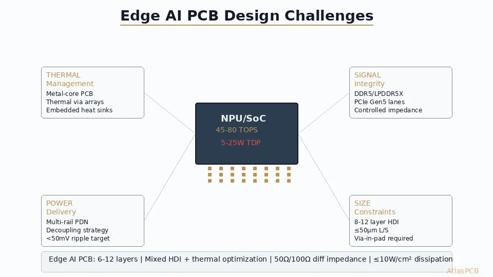
Cloud AI spreads 300-700W across large server boards (300x400mm+) with unlimited cooling budgets. Edge AI packs 50-150W into modules smaller than a credit card. This density creates three simultaneous engineering constraints:
- Thermal density: 10-30 W/cm2 concentrated under a single package with limited airflow
- Power delivery: 50-150A at 0.7-1.0V core voltage through short, low-impedance paths
- Signal integrity: LPDDR5 at 6400 MT/s and PCIe Gen5 at 32 GT/s in millimeter-scale routing lengths
All three constraints compete for the same stackup real estate. More power planes mean fewer signal layers. More thermal vias mean less routing area. Getting this balance right is the central challenge of edge AI PCB design.
AI HARDWARE PCB EXPERTISE
Designing an Edge AI Module?
AtlasPCB has fabricated boards for AI inference deployments requiring HDI, heavy copper, and controlled impedance. Up to 30 layers with 3/3 mil trace/space.
Get Engineering Review ›
Thermal Management: Via Arrays and Beyond
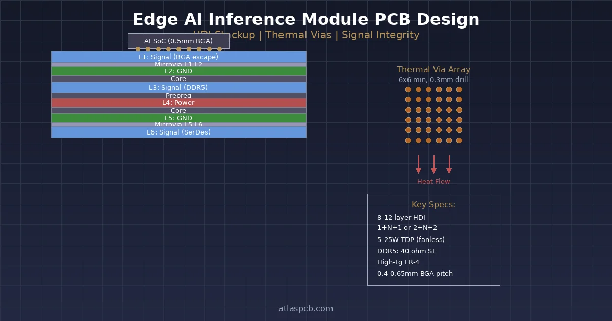
Thermal Via Array Design
For AI processors dissipating 50-150W through an exposed thermal pad:
| Design Parameter | Minimum | Recommended | Aggressive |
|---|---|---|---|
| Via drill diameter | 0.3 mm | 0.3 mm | 0.25 mm |
| Via pitch | 1.0 mm | 0.6 mm | 0.5 mm |
| Via fill | Tented | Non-conductive fill | Conductive fill |
| Thermal resistance (array) | 15 C/W | 8 C/W | 4 C/W |
Design rules:
- Fill all thermal vias (IPC-4761 Type V or VII) to prevent solder wicking during assembly
- Place vias on same grid as solder paste stencil openings to avoid paste bridging
- Connect via bottoms to a continuous copper pour on the bottom layer (heat spreader interface)
- Minimum copper connection from via to ground/power pour: full flood (no thermal relief on thermal vias)
When Via Arrays Are Not Enough
Above 100W in compact form factors (under 100x100mm), via arrays alone cannot achieve sufficient thermal resistance. Additional solutions:
- Embedded copper coin: 2-4mm thick copper slug press-fit into a milled cavity. Thermal resistance: 1-2 C/W. Adds $30-80/board.
- Metal-core layer: Aluminum or copper core layer in the stackup center. Good for uniform heat spreading across the board area.
- Direct die attach: Skips the package thermal interface — die bonded directly to board-level heat spreader. Requires bare die assembly capability.
Power Delivery Network Design
The Edge AI PDN Challenge
A typical edge AI ASIC draws:
- Core: 50-100A at 0.75V (VDD)
- I/O: 10-20A at 1.2V (VDDIO)
- Memory: 5-10A at 1.1V (VDDQ)
At these currents, every milliohm of PDN impedance translates to millivolts of droop. With 5% tolerance on 0.75V core supply, total PDN impedance budget is just 0.375 mOhm — including VRM, decoupling, and PCB planes combined.
PDN Stackup Strategy
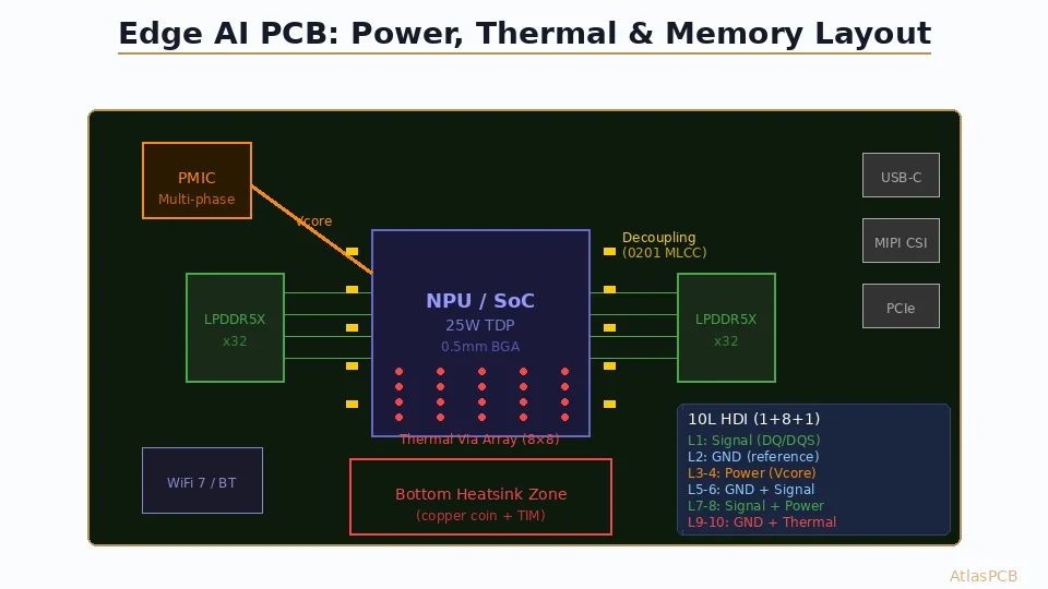
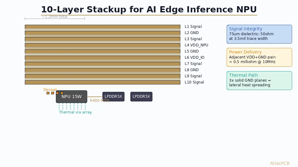
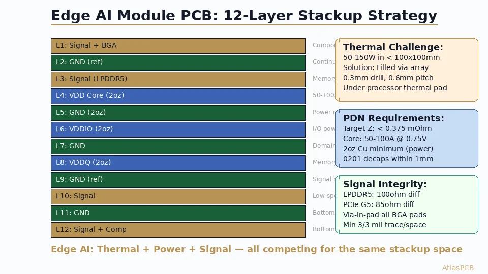
For a 12-layer edge AI module:
| Layer | Function | Cu Weight | Notes |
|---|---|---|---|
| L1 | Signal + component | 1 oz | BGA fanout, passive placement |
| L2 | Ground (ref) | 1 oz | Continuous pour, signal reference |
| L3 | Signal (memory) | 0.5 oz | LPDDR5 byte lanes |
| L4 | Power (VDD core) | 2 oz | Solid pour, max area |
| L5 | Ground | 2 oz | Power return, thermal spreading |
| L6 | Power (VDDIO) | 2 oz | I/O and memory power |
| L7 | Ground | 2 oz | Isolation between domains |
| L8 | Power (VDDQ) | 2 oz | Memory power, separate domain |
| L9 | Ground | 1 oz | Signal reference |
| L10 | Signal | 0.5 oz | Low-speed I/O, misc routing |
| L11 | Ground | 1 oz | Bottom reference |
| L12 | Signal + component | 1 oz | Bottom-side passives, connectors |
Key principles:
- Every signal layer immediately adjacent to a ground plane (no signal-signal adjacent)
- Power planes sized for current density: min 2oz for 50A+ total
- Separate ground plane between analog and digital power domains
- Decoupling capacitor placement: first tier (0201) within 1mm of BGA power balls, second tier (0402) within 5mm
HEAVY COPPER + HDI
Up to 5oz Copper with 3/3 mil HDI
AtlasPCB combines heavy copper power planes with fine-line HDI signal routing in the same stackup — exactly what AI modules demand.
View Full Capabilities ›Signal Integrity: Memory and High-Speed Interfaces
LPDDR5/5X Routing Requirements
| Parameter | LPDDR5 (6400 MT/s) | LPDDR5X (8533 MT/s) |
|---|---|---|
| Impedance (single-ended) | 40-50 ohm | 40-50 ohm |
| Impedance (differential) | 80-100 ohm | 80-100 ohm |
| Max trace length | 25 mm | 20 mm |
| Length matching (intra-byte) | +/- 0.5 mm | +/- 0.25 mm |
| Length matching (inter-byte) | +/- 2 mm | +/- 1 mm |
| Routing layer | Stripline (preferred) | Stripline (mandatory) |
| Crosstalk budget | < -30 dB | < -35 dB |
| Dielectric (Dk) | Standard FR-4 OK | Low-Dk preferred |
PCIe Gen5 Routing
For the host interface (typically PCIe Gen5 x8 or x16 to the edge AI module):
- 85 ohm differential impedance (+/- 10%)
- Maximum trace length: 200mm (connector-to-connector)
- Pair-to-pair skew: < 5 mm
- Via stub: < 8 mil (backdrilling required for through-hole vias)
- Loss budget: < 8 dB at 16 GHz Nyquist
HDI Strategy for BGA Fanout
Modern edge AI processors use 0.5-0.65mm pitch BGAs with 600-2000+ balls. Fanout requires:
- Layer 1-2 microvias for signal escape from inner BGA rows
- Stacked microvias (2-3 levels) for power/ground connections to inner planes
- Via-in-pad on all BGA pads (IPC-4761 Type VII)
- 3/3 mil trace/space minimum for signal routing between via pads
Typical HDI structure: 2+N+2 or 3+N+3 buildup with 0.1mm laser-drilled microvias.
HDI FOR AI
5+N+5 HDI with Stacked Microvias
Our HDI process supports the fine-pitch BGA fanout that edge AI processors require — laser drill to 0.075mm, via-in-pad, and stacked configurations.
Explore HDI Options ›Material Selection for Edge AI Boards
| Application Tier | Material | Dk (10 GHz) | Df (10 GHz) | Tg | Use Case |
|---|---|---|---|---|---|
| Standard | High-Tg FR-4 (Tg170+) | 4.2 | 0.018 | 170C | LPDDR4, PCIe Gen4 |
| Mid-range | Megtron 4 / Tachyon 60G | 3.8 | 0.008 | 200C | LPDDR5, PCIe Gen5 |
| High-end | Megtron 6 / Tachyon 100G | 3.6 | 0.004 | 210C | LPDDR5X, 112G SerDes |
Practical guidance:
- For designs under 10 Gbps per lane: standard high-Tg FR-4 is sufficient and cheapest
- For 10-25 Gbps (PCIe Gen5, LPDDR5): mid-range materials provide adequate margin
- For 25+ Gbps (112G SerDes, LPDDR5X): high-end materials are mandatory
Most edge AI modules in 2026 operate at the mid-range tier — LPDDR5 memory and PCIe Gen5 host interface are well served by Megtron 4 class materials without needing ultra-premium laminates.
Design Checklist: Edge AI Module PCB
- Stackup: minimum 8 layers; 12+ for complex designs. Every signal layer referenced to ground.
- Power planes: 2oz minimum for core voltage. Separate domains for VDD, VDDIO, VDDQ.
- Thermal vias: Filled array under processor thermal pad, 0.3mm drill, 0.6mm pitch minimum.
- HDI: Via-in-pad for BGA, 2+N+2 minimum buildup for 0.5mm pitch packages.
- Memory routing: Stripline on layers adjacent to ground. Length-matched within +/- 0.5mm (byte).
- PCIe routing: 85 ohm differential, backdrilled vias if through-hole used.
- Decoupling: 0201 capacitors within 1mm of power balls, bulk capacitors within 5mm.
- Board thickness: 1.6-2.0mm typical. Thicker boards need backdrill consideration.
- Surface finish: ENIG for BGA reliability; consider Immersion Silver for loss-sensitive pads.
- Testing: Impedance coupon, thermal cycling validation per IPC-6012 Class 3.
ATLASPCB
Ready to Build Your Edge AI Board?
From stackup consultation to final delivery — we support the full complexity of AI hardware PCBs. Upload your design for engineering review and quote.
Get Instant Quote ›
Related Reading:
About AtlasPCB — We specialize in complex PCB manufacturing for HDI, RF, and high-reliability applications. Explore our HDI PCB manufacturing capabilities, or get an aluminum and metal-core PCB services . Every order includes free engineering review. Get your quote.
Reviewed by AtlasPCB Engineering Team — IPC-certified manufacturing specialists with 15+ years of production experience in HDI, RF, and high-reliability PCB fabrication. Content based on factory floor data and real customer design reviews.
Frequently Asked Questions
How many PCB layers do edge AI modules need?
What thermal via design works for AI chips?
What copper weight is needed for AI inference PCBs?
How do you route LPDDR5 for edge AI?
- edge AI
- PCB design
- thermal management
- power delivery
- HDI