· Marcus Lin · Engineering · 9 min read
PCB Requirements for AI Training Server Blades
Complete PCB specification guide for AI/ML training server blades carrying 56G PAM4 SerDes, HBM3 memory interfaces, and 3000W+ power delivery networks. Covers material selection, stackup architecture, power plane design, and thermal via strategies specific to GPU/TPU accelerator cards.
Quick Answer
AI training server blade PCBs require 16-24 layers with dedicated low-loss material (Megtron 6 or equivalent, Df less than 0.004 at 14 GHz) for 56G PAM4 signal integrity, 3-5oz copper inner planes for 800-3000A aggregate power delivery, and thermal via arrays dissipating 15-25 W/cm2 from GPU/TPU packages. The critical fabrication challenges are maintaining ±5% impedance on thin dielectrics (3-4 mil) while processing heavy copper power planes in the same stackup — requiring manufacturers with both RF-grade signal layer capability and heavy copper processing experience.
The PCB Challenge: Where RF Meets Power Electronics
AI training server PCBs represent perhaps the most demanding convergence of requirements in modern electronics manufacturing. A single board must simultaneously deliver:
- Signal integrity rivaling RF boards: 56G PAM4 channels with loss budgets measured in tenths of a dB per inch, requiring low-loss materials and ±5% impedance control on 3-4 mil dielectrics
- Power delivery rivaling industrial motor drives: 800-3000A aggregate current at multiple voltage rails, requiring 3-5oz copper with thermal management
- Routing density rivaling smartphone HDI: BGA breakout from 0.8mm pitch GPU packages with 4000+ pins, requiring microvias and fine line/space
No other application demands all three simultaneously at this level. The result is a PCB that costs $800-2500 per board in production quantities — driven by material cost (Megtron 6 at $60-100/sqft versus $8-12 for FR-4), heavy copper processing surcharges, and the specialized fabrication expertise required to deliver all three requirements in one stackup.
In our facility, AI server boards have grown from zero to approximately 18% of revenue in the past 18 months. The learning curve was steep — the combination of heavy copper processing (which requires extended etch times that thin fine traces on signal layers) with low-loss material impedance control (which requires precision etch to hit tight trace widths) creates conflicting process demands that required significant process development to resolve.
Material Selection: Why Standard FR-4 Cannot Work
The fundamental limitation for AI server PCBs is signal loss. 56G PAM4 modulation encodes two bits per symbol at 28 GBaud, meaning the signal bandwidth extends to 28 GHz (Nyquist). At these frequencies, the dielectric loss tangent of the PCB laminate directly determines the maximum viable channel length.
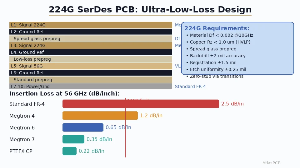
Standard FR-4 (Df approximately 0.020 at 10 GHz) produces insertion loss of approximately 1.0-1.2 dB/inch at 14 GHz. For a typical GPU-to-switch channel of 8-12 inches on a server blade, total PCB loss would reach 8-14 dB — far beyond the 15-20 dB total channel budget that includes connector loss, package routing, and silicon receiver sensitivity. The channel simply cannot close.
Megtron 6 (Df approximately 0.002 at 12 GHz) reduces per-inch loss to approximately 0.3-0.4 dB/inch at 14 GHz, enabling 8-12 inch channels within budget. The material also provides more stable Dk across frequency (3.3-3.4 from 1-20 GHz versus FR-4’s 4.7 to 4.2 drift), which simplifies impedance design and reduces mode conversion on differential pairs.
The fabrication implication is significant: Megtron 6 and similar low-loss materials require modified processing parameters compared to FR-4. Drill parameters must be adjusted (lower feed rates to prevent delamination), lamination profiles need longer press cycles (the resin system has different flow characteristics), and etch chemistry requires rebalancing because the glass weave and resin composition affect copper adhesion differently than standard FR-4.
HIGH-SPEED + HEAVY COPPER
AI Server PCB Fabrication Expertise
Low-loss Megtron 6 processing with 3-5oz copper power planes in a single stackup. ±5% impedance control on 56G PAM4 channels.
Discuss Your AI Board ›
Stackup Architecture: Balancing Signal and Power
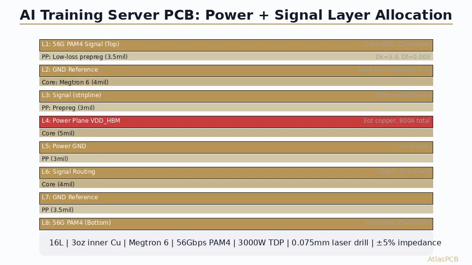
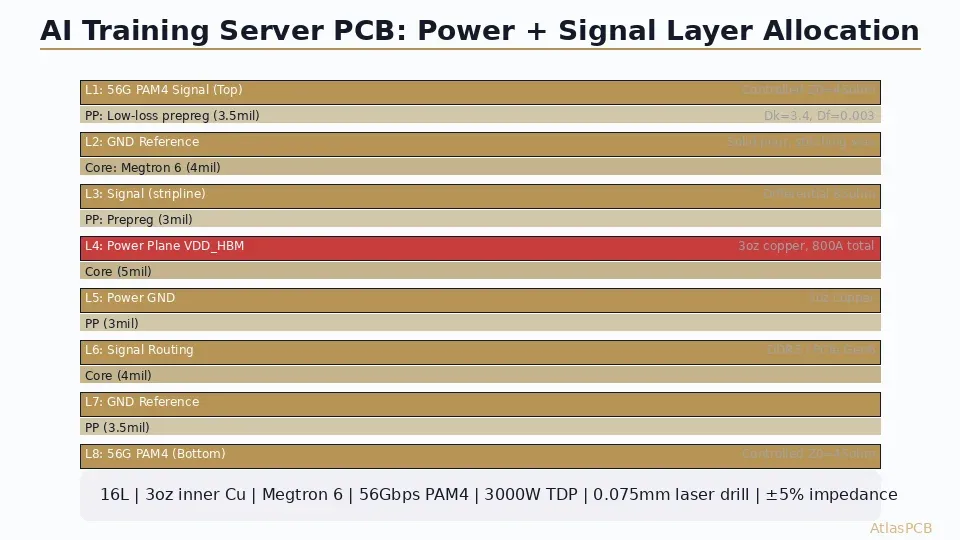
A representative 18-layer AI server blade stackup allocates layers as follows:
| Layer | Function | Copper Weight | Material |
|---|---|---|---|
| L1 | Top signal (56G PAM4 TX) | 1oz | — |
| PP | Low-loss prepreg | — | Megtron 6, 3.5mil |
| L2 | GND reference | 1oz | — |
| Core | Low-loss core | — | Megtron 6, 4mil |
| L3 | Signal (differential stripline) | 1oz | — |
| PP | Prepreg | — | 3mil |
| L4 | Power (VDD_GPU, 0.8V) | 3oz | — |
| Core | Standard core | — | 5mil |
| L5 | GND | 3oz | — |
| PP | Prepreg | — | 3mil |
| L6 | Signal routing (DDR5, misc) | 1oz | — |
| Core | Core | — | 4mil |
| L7 | Power (12V input) | 3oz | — |
| PP | Prepreg | — | 3mil |
| L8 | GND | 3oz | — |
| Core | Low-loss core | — | Megtron 6, 4mil |
| L9 | Signal (56G PAM4 RX) | 1oz | — |
| PP | Low-loss prepreg | — | Megtron 6, 3.5mil |
| L10 | Bottom signal / component | 1oz | — |
The key design principle is that 56G PAM4 channels run only on the outer signal layers (L1, L3, L9, L10) referenced to immediately adjacent ground planes, with low-loss material used specifically in these signal-to-reference layer pairs. The inner power planes use standard (cheaper) prepreg between them because no high-speed signals route on those layers. This “hybrid” approach — low-loss material where needed, standard material elsewhere — saves 25-35% on material cost compared to full-stack Megtron 6.
The heavy copper power layers (3oz on L4, L5, L7, L8) present the primary fabrication challenge. Processing 3oz copper alongside 1oz signal layers requires careful etch parameter management: the extended etch time needed to pattern 3oz copper must not over-etch the 1oz layers processed in the same panel. Our solution is sequential etch processing — inner layers are etched separately by copper weight before lamination, eliminating the conflict.
Power Delivery Network: 800A Through a PCB
The power delivery challenge on AI server blades is staggering by PCB standards. A single GPU drawing 700W at 0.8V requires 875A of current — delivered through the PCB’s power planes from VRM modules to the GPU package. Even with multiple parallel VRM phases, the current density in the power plane directly beneath the GPU can exceed 30A per square inch.
At 3oz copper (105um thickness), DC resistance per square of power plane is approximately 0.16 milliohms. For a 50mm current path from VRM to GPU, the IR drop across the plane is roughly 5mV at 875A — acceptable for a 0.8V rail where the tolerance budget is typically ±3% (24mV). Drop 5oz copper into the same design and IR drop falls to 3mV, providing more margin for transient response.
The via array connecting the GPU power pads to the internal power planes is equally critical. Each 0.3mm plated via carries approximately 3-5A reliably (based on IPC-2152 current capacity curves for 1oz barrel plating in a 1.6mm board). To deliver 875A from a power plane to the GPU, you need 175-290 power vias — which at 1.0mm pitch consumes 175-290 mm2 of pad area. This via field competes directly with signal escape routing from the GPU BGA, creating the design density challenge that pushes these boards toward HDI construction.
Thermal via arrays serve a dual purpose: conducting heat from the GPU package through the board to the heatsink mounting on the opposite side, while also providing additional current-carrying capacity for power delivery. In our standard recommendation for AI server boards, we specify 0.3mm thermal/power vias on 1.0mm pitch within the GPU footprint, transitioning to 0.5mm signal vias outside the power zone.
POWER + SIGNAL INTEGRITY
Up to 30 Layers with 5oz Copper Power Planes
Heavy copper processing combined with low-loss material impedance control in a single manufacturing flow. We handle the conflicting requirements so your SI team gets clean channels and your power team gets low impedance planes.
Fabrication Challenges Unique to AI Server Boards
Impedance Control on Thin Dielectrics with Heavy Copper Neighbors
The fundamental process conflict in AI server board fabrication is this: 56G PAM4 traces on outer layers require precise etch control (±0.5mil trace width tolerance to maintain ±5% impedance), while 3oz power planes four layers away require aggressive etch (extended time, higher concentration) that generates etchant splash-back and process chemistry loading.
If both copper weights are processed in the same etch chamber sequentially, the chemistry becomes loaded with dissolved copper from the heavy layers, changing etch rate and uniformity for subsequent light layers. The solution — which not all manufacturers implement — is dedicated etch lines or complete chemistry replacement between copper weight groups.
In our process, we sequence inner layer etching by copper weight: all 3oz layers are etched first in dedicated equipment, then the line is cleaned and chemistry rebalanced before 1oz signal layers are processed. This adds approximately 4 hours to the manufacturing cycle but ensures that signal layer trace width stays within the ±0.5mil window required for impedance compliance.
Drill Aspect Ratio on Thick Boards
An 18-layer AI server board with multiple 3oz copper layers and low-loss cores typically has a total thickness of 2.8-3.5mm. Mechanical drill through-holes at 0.25mm diameter in a 3.5mm board yields an aspect ratio of 14:1 — near the limit of reliable plating. Beyond 12:1, copper throwing power in the via barrel decreases, creating thin spots mid-barrel that become reliability concerns under thermal cycling.
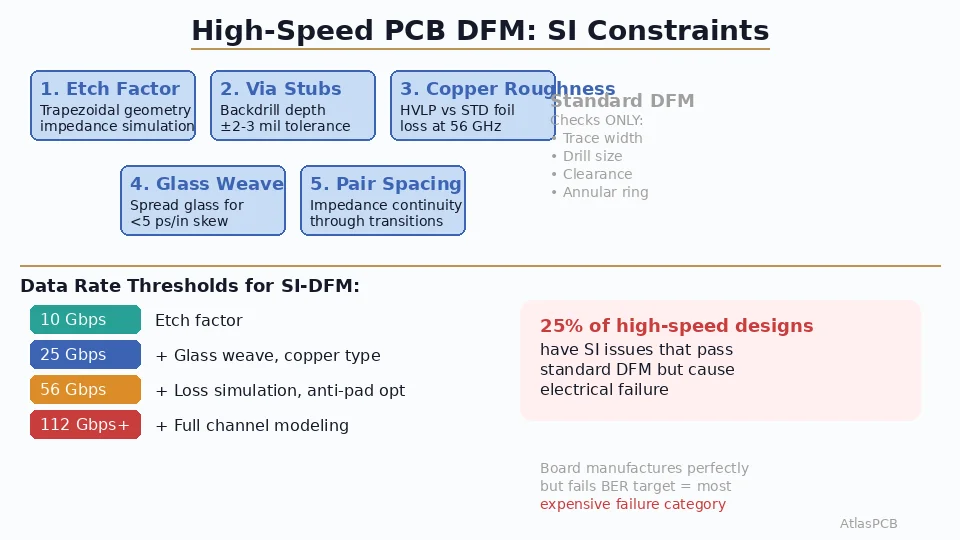
The standard approach is back-drill (controlled-depth drilling from one or both sides after plating) to remove unused via stubs that degrade signal integrity. For 56G PAM4 channels, via stubs longer than 10 mils cause measurable reflection and mode conversion. Our back-drill process achieves stub length below 8 mils (±3 mil accuracy), verified by cross-section on every production lot.
Registration Across Heavy Copper Layers
3oz copper layers are thicker and stiffer than standard 1oz layers, which affects their dimensional stability during lamination. The core material deforms less under press pressure when thick copper is present on both sides, but the differential between heavy and light copper regions creates localized registration shifts at feature boundaries.
For AI server boards where HDI microvias on outer layers must align to inner layer features, this registration shift is accounted for in our compensation algorithms — applying position offsets to the HDI drill program based on measured core layer shift data from process characterization panels.
Specification Summary for AI Training Server PCBs
| Parameter | Typical Specification | AtlasPCB Capability |
|---|---|---|
| Layer count | 16-24 | Up to 30 |
| Signal material | Megtron 6, Dk 3.4, Df 0.002 | Yes |
| Power plane copper | 3-5oz | Up to 5oz inner |
| Impedance tolerance | ±5% on low-loss layers | ±5% verified by TDR |
| Min trace/space (signal) | 3.5/3.5 mil (89/89 um) | 3/3 mil (75/75 um) |
| Backdrilling | Stub < 10 mil | Stub < 8 mil, ±3 mil |
| Via aspect ratio | 12-14:1 | Up to 16:1 |
| Thermal via pitch | 1.0mm | 0.8mm minimum |
| Board thickness | 2.8-3.5mm | 0.2-5.5mm range |
| ENIG finish | For GPU BGA pads | Yes, with selective options |
ATLASPCB
Building AI Hardware? Let's Talk PCB Specs.
We fabricate 16-30 layer boards with low-loss materials and heavy copper power planes for AI accelerator programs. Upload your design or stackup concept for engineering review and feasibility assessment.
Get Engineering Review ›
Reviewed by AtlasPCB Engineering Team — 15+ years in advanced PCB fabrication for RF, HDI, and rigid-flex applications.
Related Reading:
About AtlasPCB — We specialize in complex PCB manufacturing for HDI, RF, and high-reliability applications. Explore our HDI PCB manufacturing capabilities, RF and high-frequency PCB services, or get an impedance-controlled PCB manufacturing . Every order includes free engineering review. Get your quote.
Reviewed by AtlasPCB Engineering Team — IPC-certified manufacturing specialists with 15+ years of production experience in HDI, RF, and high-reliability PCB fabrication. Content based on factory floor data and real customer design reviews.
Frequently Asked Questions
What PCB material is required for 56G PAM4 signal integrity?
How much copper do AI server PCB power planes need?
What layer count is typical for AI training server PCBs?
What are the thermal management challenges for AI server PCBs?
Can a standard PCB manufacturer fabricate AI server boards?
- RF PCB design and manufacturing
- HDI PCB manufacturer
- AI hardware PCB
- high-speed PCB
- power delivery network