· Marcus Lin · Engineering · 11 min read
5G Antenna PCB Fabrication: Material Via
A fabrication-focused guide to 5G antenna PCBs — covering material selection for sub-6 GHz vs mmWave bands, via transition design for feed networks, antenna-in-package substrate requirements, and the manufacturing constraints that determine whether your phased array design is producible.
Quick Answer
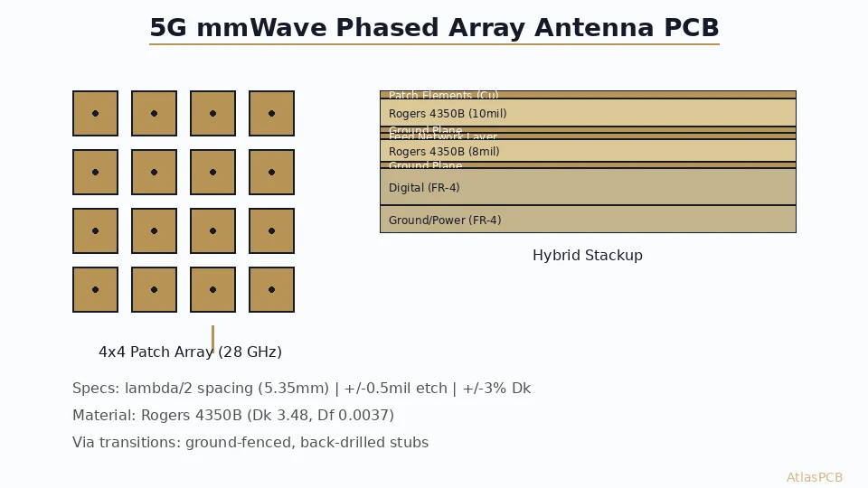
5G antenna PCB fabrication requires material selection matched to the operating band: standard Rogers 4350B (Dk 3.48, Df 0.0037) works for sub-6 GHz and n77/n78 bands, while mmWave frequencies above 24 GHz demand RO3003 (Dk 3.0, Df 0.0013) or PTFE-based substrates for acceptable antenna efficiency. The critical manufacturing challenges are via transition impedance control in the feed network, patch element dimensional accuracy (+/-0.5mil tolerance for 28 GHz patches), and maintaining consistent dielectric thickness across the antenna aperture for uniform beam performance.
5G Antenna PCB: Band-by-Band Material Selection
| 5G Band | Frequency | Recommended Material | Dk | Df | Patch Size (approx) | Key Challenge |
|---|---|---|---|---|---|---|
| n77/n78 (Sub-6) | 3.3-4.2 GHz | Rogers 4350B | 3.48 | 0.0037 | 24mm x 24mm | Feed network length |
| n257/n261 (mmWave) | 26.5-29.5 GHz | Rogers 4350B or RO3003 | 3.48 / 3.0 | 0.0037 / 0.0013 | 3.5mm x 3.5mm | Patch dimensional accuracy |
| n260 (mmWave) | 37-40 GHz | RO3003 or Taconic TLY-5 | 3.0 / 2.2 | 0.0013 / 0.0009 | 2.5mm x 2.5mm | Via transition loss + patch tolerance |
| n262 (mmWave) | 47.2-48.2 GHz | PTFE (RO3003 min) | 3.0 | 0.0013 | 2.1mm x 2.1mm | Material isotropy, etch uniformity |
The material decision is not purely about dielectric loss — it also determines antenna bandwidth. Higher-Dk materials (like RO4350B at 3.48) produce narrower bandwidth per element, which may be acceptable for single-band operation but limits designs targeting multiple mmWave bands simultaneously. Lower-Dk materials (RO3003, TLY-5) provide 15-30% wider element bandwidth at the cost of larger element footprint.
Feed Network Design: Where Fabrication Meets RF Performance
The corporate feed network distributes signal from the transceiver IC to every antenna element in the array. In a 64-element phased array, this network comprises 63 power dividers, each requiring impedance-matched transmission lines and (in multi-layer designs) via transitions between routing layers. The fabrication quality of this feed network directly determines the array’s radiation efficiency, sidelobe level, and beam-pointing accuracy.
For planar (single-layer) feed networks using microstrip, the critical fabrication parameter is trace width uniformity across the full array aperture. A 50-ohm microstrip on 10mil Rogers 4350B requires approximately 22mil trace width. If etch variation causes this width to fluctuate by +/-1mil across the panel, the impedance changes by approximately +/-2.5 ohms — acceptable for most array applications. However, if the variation is systematic (thicker etch on panel edges versus center), it creates amplitude taper errors that distort the radiation pattern.
Our process monitors etch uniformity at 9 points across the panel during production, holding trace width to +/-0.5mil for antenna boards. This is tighter than standard impedance-controlled work (+/-1mil) because antenna performance is more sensitive to amplitude and phase uniformity across elements than typical digital impedance budgets.
For multi-layer feed networks (common in arrays with dual polarization or beamforming subnets), via transitions become the dominant loss mechanism. Each transition from a microstrip on the antenna layer through a via to a stripline on an inner routing layer introduces a mode conversion that, if poorly optimized, radiates energy into the parallel-plate mode between ground planes rather than coupling to the target transmission line.
CHINA RF PCB MANUFACTURER
5G Antenna PCBs with +/-0.5mil Etch Tolerance
LDI patterning, Rogers/PTFE material expertise, and antenna-grade etch uniformity across the full array aperture. From single prototypes to volume production.
Get RF PCB Quote ›
Via Transition Optimization: The 3 dB Difference
An unoptimized signal via at 28 GHz typically shows 15 dB return loss and 0.3 dB insertion loss — meaning 3% of signal power reflects back and 7% is radiated or absorbed. For a single transition this is manageable, but arrays require 2 transitions per element (down from antenna layer to routing layer, then back up to the next element group). In a 64-element array with a corporate feed, there are approximately 126 via transitions in the signal path from input to the farthest element.
At 0.3 dB per transition, the cumulative feed network loss reaches 4-5 dB on the longest path — devastating for array efficiency. Optimized via transitions reduce this to 0.05-0.08 dB each, bringing total via-related loss to under 1 dB.
Three fabrication techniques enable optimized via transitions:
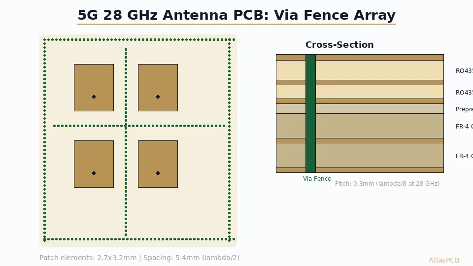
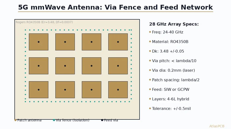
Ground via fencing places 4-8 ground vias in a ring around the signal via, forming a coaxial-like structure that suppresses parallel-plate mode radiation. The critical dimension is the ground via distance from the signal via — typically 8-15mil spacing at 28 GHz, requiring accurate drill registration relative to the signal via. Our CNC machines achieve +/-2mil via-to-via position accuracy, which provides adequate control for ground fence placement up to 40 GHz.
Anti-pad diameter tuning adjusts the non-functional clearance on ground planes to compensate the via’s excess capacitance. The optimal anti-pad diameter is typically 20-30mil for a 12mil signal via at 28 GHz — larger than the standard 24mil default in most CAD tools. This requires custom pad stack definitions that many designers overlook.
Back-drill stub removal eliminates the via stub extending below the target layer. At 28 GHz, a 20mil via stub creates a quarter-wave resonance that produces a notch in the transmission response. Our back-drill process removes stubs to within +/-3mil of the target layer, eliminating this resonance. For designs where back-drilling is not feasible (blind vias, sequential lamination builds), via depth must be controlled by stackup design instead.
Patch Element Manufacturing: Dimensional Control at mmWave
At microwave frequencies, the patch antenna element dimension directly determines its resonant frequency. The relationship is approximately linear: a 1% error in patch width creates a 1% error in resonant frequency. At 28 GHz, the 5G NR channel bandwidth for n257 is 400 MHz (26.5-29.5 GHz), and the element bandwidth on Rogers 4350B is approximately 800-1000 MHz (3-4%). This means a 1% dimensional error shifts the element tuning by 280 MHz — consuming a significant fraction of the operational bandwidth margin.
The fabrication challenge is maintaining patch dimensions within +/-0.5% across an array that may span 50-100mm in each direction. This requires not just accurate patterning (which LDI provides at +/-15um) but also uniform etching across the entire array area. Edge effects in spray etch systems cause 0.5-1mil additional etch on panel perimeters compared to the center. For antenna arrays, we run panel layouts that center the antenna area and use sacrificial copper borders to absorb edge etch variation.
Equally critical is dielectric thickness uniformity beneath the patch elements. The patch resonant frequency depends on dielectric thickness as well as width — a 5% thickness variation shifts frequency by approximately 2.5%. Standard prepreg pressing achieves +/-8% thickness tolerance. For antenna applications, we specify +/-3% on the antenna layer dielectric by selecting narrow-tolerance material lots and using higher lamination pressure with precise thermal profiling.
RF PCB DESIGN AND MANUFACTURING
mmWave Antenna Arrays with LDI Patterning
+/-15um feature accuracy on Rogers and PTFE substrates. Dielectric thickness control to +/-3% for patch frequency accuracy. Prototype to volume.
Sub-6 GHz vs mmWave: Different Fabrication Challenges
Sub-6 GHz 5G antenna PCBs (bands n77, n78, n79 at 3.3-4.9 GHz) present fundamentally different manufacturing challenges than mmWave boards. At these frequencies, patch elements are large (20-25mm square) and dimensional tolerance is relaxed — +/-0.5mm is adequate for resonant frequency control within the 3GPP channel bandwidth.
The challenge at sub-6 GHz is feed network length and associated insertion loss. A massive MIMO antenna panel with 128 elements may span 600mm or more, with feed network traces running 200-400mm from the input connector to the farthest elements. Even on Rogers 4350B (Df 0.0037), a 400mm microstrip at 3.5 GHz accumulates approximately 1.5 dB of dielectric loss. Combined with conductor loss (0.3-0.5 dB for half-ounce copper at these frequencies), total feed network loss reaches 2+ dB on long paths.
The fabrication implications: sub-6 GHz panels require large-format manufacturing (our maximum panel dimension is 600x1200mm, accommodating most massive MIMO arrays in a single panel), uniform copper thickness across large areas for consistent conductor loss, and excellent layer-to-layer registration for stripline feed networks where ground plane gaps cause radiation leakage.
mmWave boards, conversely, are physically small (typically 30-80mm per array module) but demand extreme dimensional precision. The primary manufacturing challenge shifts from panel size to feature accuracy — every microstrip, via, and patch dimension directly impacts radiation performance at 28-39 GHz.
Selecting a Manufacturer for 5G Antenna PCBs
Not every PCB fabricator can produce antenna-grade boards, and the capability gap between standard impedance-controlled work and antenna fabrication is significant. When evaluating manufacturers for 5G antenna PCBs, verify these specific capabilities:
LDI (Laser Direct Imaging) is mandatory for mmWave antenna boards. Film-based imaging has feature accuracy of +/-50um — insufficient for 28 GHz patch elements requiring +/-25um. LDI achieves +/-15um, providing adequate margin. All our antenna production uses LDI on the antenna and feed network layers.
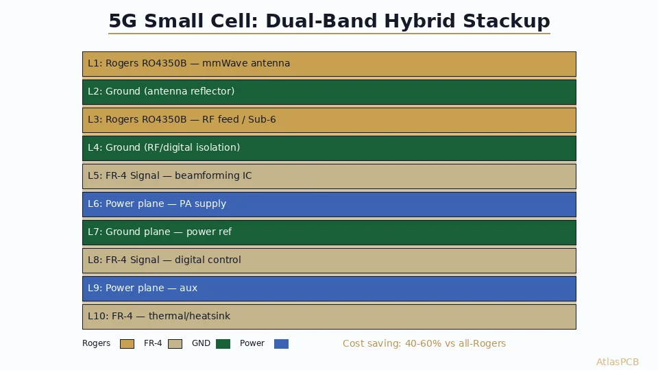
Rogers/PTFE material experience is not just about stocking the material — it includes understanding the etch characteristics (Rogers etches differently than FR-4 due to different copper adhesion profiles), drilling parameters (lower feed rates to prevent delamination at the copper-Rogers interface), and press profiles (Rogers requires precise ramp rates to achieve proper bonding without resin squeeze-out on adjacent FR-4 layers in hybrid builds).
Dielectric thickness measurement capability beyond standard caliper checks is necessary for antenna layers. We use a combination of cross-section metallography and capacitance-based thickness measurement at multiple points across the panel to verify +/-3% dielectric tolerance on antenna layers.
Antenna-specific test coupons — beyond standard impedance coupons — verify patch frequency response, feed network insertion loss, and via transition quality. Not all manufacturers have the RF test equipment or expertise to design and measure these coupons. We maintain a vector network analyzer (VNA) setup calibrated for antenna coupon characterization up to 50 GHz.
5G ANTENNA PCB SPECIALISTS
From Prototype to Volume 5G Antenna Production
LDI patterning, VNA-verified coupons to 50 GHz, and Rogers/PTFE processing experience across 1,000+ antenna panels delivered. Upload your array design.
Upload Design ›Design-for-Manufacturing: 5G Antenna-Specific Rules
Beyond standard PCB DFM, antenna boards require attention to fabrication rules that specifically impact radiation performance.
Solder mask on antenna elements must be carefully specified. Solder mask has a dielectric constant of approximately 3.3-3.8 and adds an overlay thickness of 15-25um. On a patch element designed without accounting for mask, this overlay shifts resonant frequency downward by 200-500 MHz at 28 GHz — potentially moving the antenna off-band. Two approaches work: either design the element dimensions assuming mask will be present (subtract 2-3% from calculated dimensions), or specify a mask opening (solder mask defined aperture) that removes mask from the element entirely. We recommend mask removal for mmWave patches to eliminate the uncertainty.
Edge plating and board profile tolerance matter for antenna elements near board edges. A patch element within 5mm of the board edge experiences ground plane truncation that distorts its radiation pattern. The board edge also needs clean profiling (routing, not V-score) to avoid copper burrs that create spurious radiation. Specify routing with 6mil edge-to-copper clearance minimum.
Panel array registration for multi-board antenna systems requires matching element positions across multiple PCBs that are assembled into a larger array. If boards are misaligned when stacked, the effective inter-element spacing varies, creating beam-pointing errors. We support fiducial-referenced panel positioning with +/-2mil board-to-board registration accuracy for multi-board array assemblies.
ATLASPCB
Building a 5G Antenna System? Start with the Right PCB.
Sub-6 GHz massive MIMO or mmWave phased array — our RF team has the material stock, process capability, and test infrastructure for antenna-grade fabrication.
Get Antenna PCB Quote ›
Reviewed by AtlasPCB Engineering Team — 15+ years in advanced PCB fabrication for RF, HDI, and rigid-flex applications.
Related Reading:
About AtlasPCB — We specialize in complex PCB manufacturing for HDI, RF, and high-reliability applications. Explore our RF and high-frequency PCB services, Rogers RO4350B PCB manufacturing, or get an impedance-controlled PCB manufacturing . Every order includes free engineering review. Get your quote.
Reviewed by AtlasPCB Engineering Team — IPC-certified manufacturing specialists with 15+ years of production experience in HDI, RF, and high-reliability PCB fabrication. Content based on factory floor data and real customer design reviews.
Frequently Asked Questions
What PCB material should I use for a 5G antenna at 28 GHz?
What dimensional tolerance do 5G mmWave patch antennas require?
Can a standard PCB manufacturer fabricate 5G antenna boards?
How do via transitions affect 5G antenna PCB performance?
What is the minimum element spacing for a 5G mmWave antenna array?
- 5G antenna PCB fabrication
- RF PCB design and manufacturing
- Rogers 4350B stackup
- China RF PCB manufacturer
- impedance controlled PCB