· AtlasPCB Engineering Team · News · 3 min read
Infineon Leads €120M Moore4Power Project
A European consortium led by Infineon has launched Moore4Power — a €120 million research project combining silicon, silicon carbide, and gallium nitride power devices with sensing and communication on heterogeneously integrated substrates.
Key Takeaway
Infineon Technologies is leading Moore4Power, a newly launched European research initiative with over €120 million in combined funding, aimed at combining silicon (Si), silicon carbide (SiC), and gallium nitride (GaN) power devices together with sensing, control, and communication functions on single heterogeneously integrated system modules.
The project, announced on May 22, 2026, represents a major step toward “More than Moore” integration in power electronics — and creates significant new requirements for the PCB and substrate technologies that support these advanced modules.
Project Scope and Goals
Moore4Power’s subtitle — “More than Moore for Disruptive Innovations in Power Electronics” — signals its ambition to push beyond traditional scaling toward functional integration:
Key objectives:
- Integrate Si CMOS control with SiC/GaN power switches on common substrates
- Combine thermal sensing, current measurement, and communication interfaces alongside power paths
- Develop new substrate materials and interconnect technologies to handle >200°C junction temperatures alongside sensitive analog circuits
- Target applications in EV powertrains, renewable energy inverters, and industrial motor drives
The consortium includes major European semiconductor companies, research institutes, and substrate/packaging specialists working together through 2029.
PCB and Substrate Implications
The heterogeneous integration of power devices with digital/sensing functions on shared substrates creates new challenges directly relevant to PCB manufacturing:
Thermal Management
Combining 200°C+ SiC/GaN junctions with temperature-sensitive CMOS control circuits requires:
- Extreme thermal gradient management — local hot spots must not affect adjacent control circuits
- High-temperature substrate materials — standard FR-4 (Tg 170°C) is inadequate; polyimide, ceramic, or high-Tg thermoset substrates required
- Embedded thermal isolation — trenches, thermal vias, and material boundaries to control heat flow directionality
High-Current / High-Voltage Coexistence
Power modules switching 800V at 100A adjacent to 3.3V sensing circuits require:
- Heavy copper (4–10 oz) on power layers with fine-line (3 mil) on signal layers in the same board
- Isolation distances per IEC 61800 and UL 840 within the substrate itself
- Partial discharge resistance of dielectric materials at field strengths approaching 20 kV/mm
Mixed-Signal Integrity
Communication interfaces (CAN FD, Ethernet) operating alongside multi-MHz switching noise demand:
- Shielded routing within the module substrate
- Ground plane partitioning with controlled common-mode current paths
- EMI containment through via fencing and embedded shields
Industry Context
Moore4Power joins a growing ecosystem of European initiatives to build advanced packaging and substrate capabilities:
- EDIP (European Defence Industry Programme): Includes PCB and substrate supply chain security
- EU Chips Act: €43 billion for semiconductor ecosystem, including advanced packaging
- Fraunhofer ISIT/IZM: Active in panel-level packaging and embedding research
The project’s substrate requirements may accelerate development of:
- Copper-invar-copper (CIC) core PCBs for CTE matching with SiC
- Aluminum nitride (AlN) hybrid substrates with organic redistribution layers
- Embedded die technology for integrating GaN HEMTs within PCB layers
What This Means for PCB Manufacturers
Moore4Power signals that the next generation of power modules will demand PCB substrate capabilities currently found only in IC packaging:
- Multi-level copper weight on single boards (2 oz signal + 10 oz power)
- High-temperature materials with Tg > 250°C and Td > 350°C
- Partial discharge testing as a standard inspection requirement
- Tighter registration between heavy copper power features and fine-pitch control routing
- Hybrid construction combining ceramic and organic substrates
At AtlasPCB, we already offer heavy copper PCB fabrication up to 6 oz and high-temperature materials for power electronics applications. As heterogeneous integration advances, we’re expanding capabilities to support the convergence of power and signal in single substrates.
Source: Semiconductor Today, May 22, 2026; Infineon Technologies AG press materials
Building power electronics PCBs that need heavy copper, high-temperature materials, or mixed copper weights? Request a quote from AtlasPCB’s power electronics team.
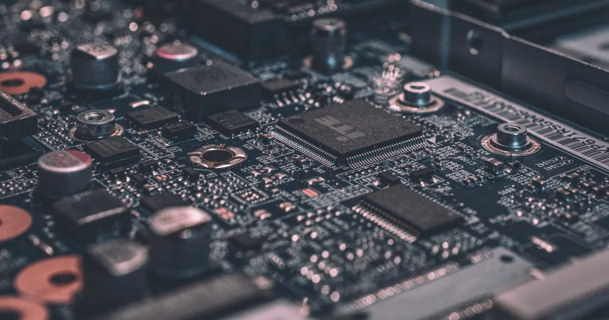
Image: Vishnu Mohanan via Unsplash
About AtlasPCB — We specialize in complex PCB manufacturing for HDI, RF, and high-reliability applications. Explore our heavy copper PCB manufacturing . Every order includes free engineering review. Get your quote.
Reviewed by AtlasPCB Engineering Team — IPC-certified manufacturing specialists with 15+ years of production experience in HDI, RF, and high-reliability PCB fabrication. Content based on factory floor data and real customer design reviews.
- news
- Infineon
- Moore4Power
- heterogeneous integration
- SiC
- GaN
- power electronics
- PCB substrate
- advanced packaging