· Thomas Webb · News · 3 min read
Electroninks Introduces Air-Curable Copper
Austin-based Electroninks announces ambient-atmosphere copper MOD ink that cures at 150°C without inert gas, enabling cost-effective large-area copper metallization for PCB and semiconductor packaging applications.
Electroninks Eliminates Inert Atmosphere Requirement for Copper Ink Curing
Austin, Texas-based Electroninks has announced a breakthrough advancement to its copper metal-organic decomposition (MOD) ink platform: a copper metallization technology capable of curing under ambient conditions, open to air, at approximately 150°C for 5 to 10 minutes.
The development addresses a fundamental limitation that has constrained copper-based conductive inks since their inception. Copper oxidizes readily at elevated temperatures, traditionally requiring nitrogen or forming gas atmospheres, vacuum equipment, or heat press systems to produce conductive films. Electroninks’ new formulation removes these infrastructure requirements entirely.
Source: PCB Directory (June 2026)
Technical Significance
The Cu-MOD ink builds on Electroninks’ September 2024 commercial launch of its copper ink platform, which demonstrated low resistivity and adhesion across multiple substrates. The air-curable advancement is significant for several reasons:
Cost reduction: Eliminating inert gas infrastructure reduces capital equipment costs for additive metallization lines by an estimated 30-40%. Large-area metallization applications particularly benefit, as maintaining nitrogen atmosphere over wide-format substrates requires substantial gas volumes.
Process compatibility: Curing at 150°C for 5-10 minutes is compatible with standard thermal processing equipment already present in PCB fabrication and assembly facilities. No specialty tooling, vacuum chambers, or lamination systems are required.
Substrate versatility: Preliminary results demonstrate performance on polyimide, glass, EMC (epoxy molding compound), and build-up film substrates — covering the primary materials used in both traditional PCB manufacturing and advanced semiconductor packaging.
“While silver and gold will remain key materials in many applications, for large area and full-film metallization, the rising cost of precious metals has renewed interest across the electronics industry in cost-effective alternatives that do not compromise electrical performance,” said Kazutaka Ozawa, Technical Director at Electroninks.
Industry Context: Additive Manufacturing in PCB Fabrication
The PCB industry has traditionally relied on subtractive processes — depositing copper across entire panel surfaces, then etching away unwanted material. This approach wastes 60-80% of the copper deposited and generates significant chemical waste. Additive and semi-additive (SAP/mSAP) processes deposit copper only where needed, offering:
- Material savings of 50-70% on copper consumption
- Reduced chemical processing steps (fewer etch baths)
- Finer feature capability (line/space below 25/25µm)
- Compatibility with flexible and novel substrates
Electroninks’ air-curable copper ink adds another option to this additive toolkit. While electroless and electrolytic copper plating remain dominant for standard PCB production, ink-based approaches offer unique advantages for:
- Rapid prototyping (print-and-cure in minutes vs. hours of wet processing)
- Repair and rework of damaged traces
- Heterogeneous integration on non-traditional substrates
- Selective metallization without photolithography masks
Market Applications and Availability
Electroninks is currently working with a select group of development partners across multiple sectors. The company expects to release full performance data, including resistivity measurements and adhesion results on production substrates, in Q3 2026.
Potential applications extend beyond traditional PCB manufacturing to include:
- Advanced packaging: Redistribution layers (RDL) on fan-out wafer-level packages
- Flexible electronics: Copper traces on polyimide flex circuits
- Display technology: Copper interconnects on glass substrates
- Automotive sensors: Direct metallization on molded interconnect devices (MID)
- EMI shielding: Selective copper deposition for compartmentalized shielding
What This Means for PCB Manufacturers
While Electroninks’ technology is still in development-partner phase, it signals a broader industry shift toward atmospheric-condition copper processing. For PCB fabricators evaluating additive manufacturing roadmaps, the elimination of inert-atmosphere requirements removes a significant barrier to adoption.
AtlasPCB continues to invest in both traditional subtractive and advanced semi-additive processing capabilities. Our mSAP process line currently achieves 30/30µm line/space for HDI and substrate-like PCB applications — contact our engineering team to discuss your fine-line manufacturing needs.
Further Reading
- PCB Copper Plating: Electroless vs Electrolytic for HDI Vias
- Flash Copper Plating for HDI Microvia and mSAP Seed Layers
- IC Substrate vs HDI: Substrate-Like PCB (SLP) Technology
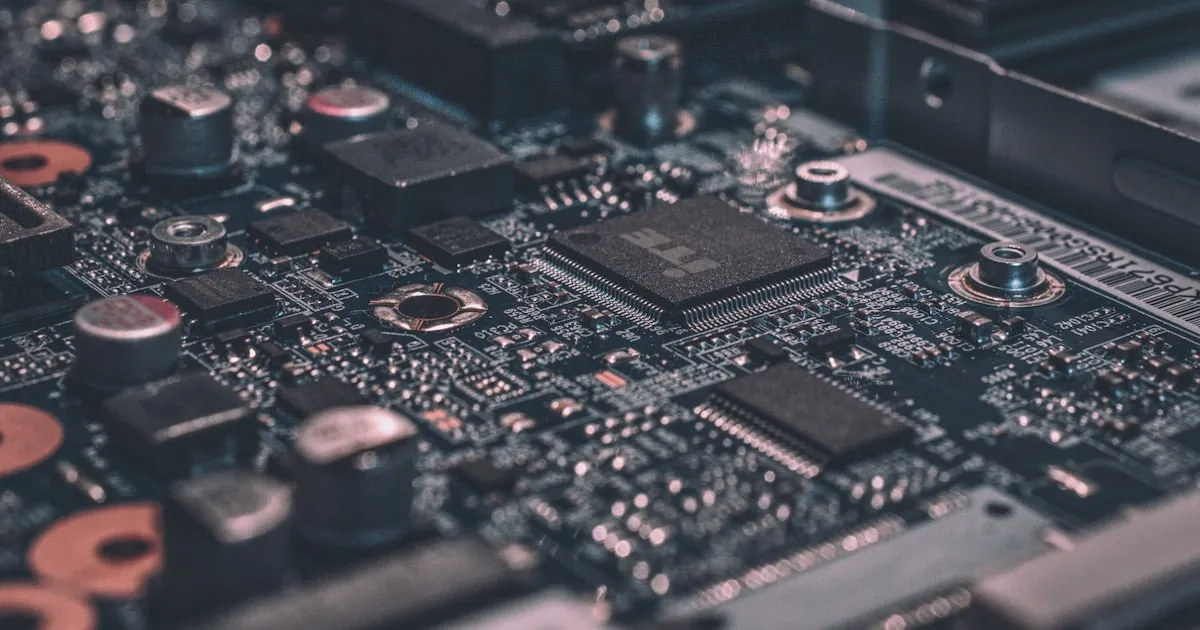
Image: Vishnu Mohanan via Unsplash
About AtlasPCB — We specialize in complex PCB manufacturing for HDI, RF, and high-reliability applications. Explore our full PCB manufacturing capabilities, or get an instant online quote . Every order includes free engineering review. Get your quote.
Reviewed by AtlasPCB Engineering Team — IPC-certified manufacturing specialists with 15+ years of production experience in HDI, RF, and high-reliability PCB fabrication. Content based on factory floor data and real customer design reviews.
- news
- additive manufacturing
- copper metallization
- PCB materials
- conductive ink
- advanced packaging