· David Okafor · Engineering · 7 min read
What Is DFM in PCB? Design for Manufacturability
A clear explanation of DFM (Design for Manufacturability) in PCB design — what it covers, why it matters, and how it prevents costly manufacturing failures.
Quick Answer
DFM (Design for Manufacturability) in PCB design is the practice of designing a circuit board so it can be reliably manufactured at a specific factory, using specific materials and processes, within specified tolerances. DFM goes beyond basic design rules (DRC) by considering real-world manufacturing constraints: available material thicknesses, factory-specific registration accuracy, etch compensation for copper weight, impedance accuracy on actual stackups, and via reliability for the board's thermal profile.
DFM stands for Design for Manufacturability. In PCB design, it means ensuring your board can actually be built — reliably, repeatedly, and within specification — by a real factory with real equipment and real material constraints.
It is not the same as DRC. It is not a software feature. It is an engineering discipline that bridges the gap between what your CAD tool allows and what a factory can produce.
DFM vs DRC: They Are Not the Same Thing
This distinction matters because many designers assume that passing DRC means their design is manufacturable. It does not.
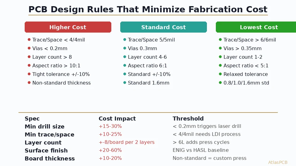
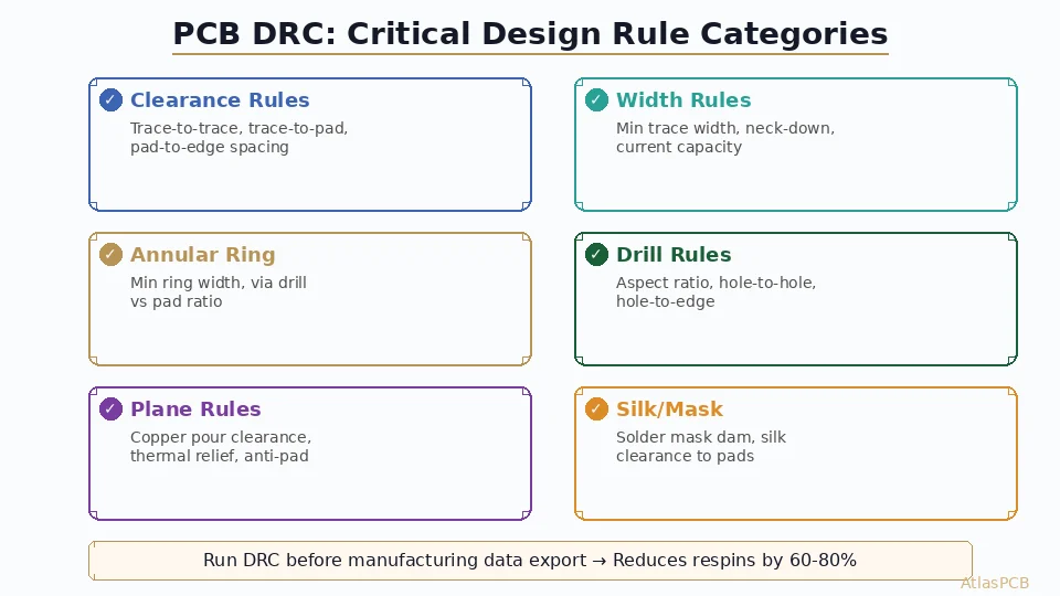
| Aspect | DRC (Design Rule Check) | DFM (Design for Manufacturability) |
|---|---|---|
| What it checks | Geometric rules | Manufacturing feasibility |
| How it runs | Automated software | Human engineering review |
| Speed | Seconds to minutes | Hours (4-12 for complex boards) |
| Catches | Rule violations | Process-specific problems |
| Misses | Material availability, impedance accuracy, thermal behavior, factory-specific limits | Nothing (if done thoroughly) |
| When to run | Every design iteration | Before final Gerber submission |
Example of what DRC passes but DFM catches:
Your design has a 12-layer stackup, 1.6mm total thickness, 50Ω controlled impedance on 4 layers. DRC passes — all traces meet minimum width, all vias meet minimum drill.
DFM review finds:
- 1.6mm with 12 layers requires 2.5mil dielectrics — the factory’s thinnest prepreg is 3.5mil. Minimum achievable thickness is 2.0mm.
- 50Ω requires 4.8mil trace on the actual dielectric, but the design has 5.5mil traces — impedance will be 45.2Ω, outside ±5%.
- Layer 6-7 have 85% copper density while layers 1-2 have 20% — the board will warp 1.8%, exceeding the 0.75% Class 3 limit.
All three issues are invisible to DRC. All three cause the board to fail.
What DFM Covers
1. Stackup Manufacturability
Your stackup must be buildable with materials the factory actually stocks or can source. DFM checks:
- Dielectric thicknesses match available prepreg and core options
- Total board thickness is achievable with the specified layer count
- Material grade is appropriate (standard Tg, mid-Tg, high-Tg based on layer count and thermal requirements)
- Sequential lamination plan (for HDI or complex multilayer) is compatible with the factory’s press equipment
2. Impedance Feasibility
DFM verifies that your trace geometry produces the target impedance on the actual stackup — not a theoretical one. This requires:
- Running the trace width through a field solver with actual Dk values
- Accounting for etch factor (traces get narrower during etching — the amount depends on copper weight)
- Including solder mask effect for microstrip traces
- Comparing calculated impedance to target ± tolerance
3. Via Manufacturability
Vias have physical limits that vary by factory:
- Aspect ratio — board thickness ÷ drill diameter must be within the factory’s capability (typically ≤10:1 standard, ≤8:1 for Class 3)
- Blind via depth — controlled-depth drilling accuracy limits how deep a blind via can reliably reach
- Microvia size — laser drill minimum depends on equipment (CO2 vs UV-YAG) and dielectric material
- Buried via span — must fall within sub-lamination boundaries
- Via fill — required for stacked microvias and via-in-pad; must be specified explicitly
4. Copper Balance
Unbalanced copper distribution causes warpage. DFM assesses:
- Per-layer copper density (ideal: all layers within 20% of each other)
- Top-to-bottom symmetry (copper weight and density should mirror around the board center)
- Local density variations (large copper-free zones adjacent to solid pours cause local stress)
5. Manufacturing Tolerance Stack
Every manufacturing step introduces variation. DFM checks whether the accumulated tolerance stays within specification:
- Drill position accuracy + lamination registration → annular ring
- Etch variation + dielectric variation → impedance tolerance
- Press thickness variation + material tolerance → total thickness
- Copper plating uniformity → trace width consistency
6. Documentation Completeness
A board without complete documentation requires the manufacturer to make assumptions. DFM verifies that your fab notes specify:
- Material and Tg rating
- Surface finish
- Impedance requirements (target, tolerance, trace type, reference layer)
- IPC class
- Special requirements (back-drill, edge plating, controlled depth routing)
- Drill file format and plated/non-plated designation
The Cost of Bad DFM
DFM problems discovered at different stages have dramatically different costs:
| Discovery Stage | Typical Cost | Time Impact |
|---|---|---|
| During design (self-review) | $0 | 0 — fix before generating Gerbers |
| During manufacturer review | $0-500 | 1-3 days for redesign |
| During manufacturing | $2,000-5,000 | 1-3 weeks (re-order + re-manufacture) |
| During assembly | $5,000-15,000 | 2-4 weeks (debug + re-spin board + re-order) |
| In the field | $20,000-500,000+ | Months (recall, investigation, redesign, requalify) |
The pattern is clear: DFM review before manufacturing is essentially free. Every later stage multiplies cost by 5-10x.
DFM Best Practices
For Designers
Know your manufacturer’s capabilities before starting layout. Request their capability sheet — minimum trace/space, drill sizes, layer count, aspect ratio, registration tolerance.
Design to the middle of the tolerance range, not the edge. If the factory’s minimum trace width is 3mil, design at 4mil. This provides margin for manufacturing variation.
Specify everything in fab notes. “FR4” is not a specification. “Shengyi S1000-2M, Tg 170°C, 1oz copper on all layers, ENIG surface finish, IPC Class 2” is a specification.
Run your own DFM check using a checklist before sending files. See our [50-point DFM checklist]/blog/pcb-dfm-checklist/) for a comprehensive list.
Send a preliminary stackup to your manufacturer before finalizing layout — especially for HDI, RF, or high-layer-count boards.
For Manufacturer Selection
Choose a manufacturer that performs human engineering review — not just automated DRC. See our guide on [engineering review]/blog/pcb-manufacturer-engineering-review/).
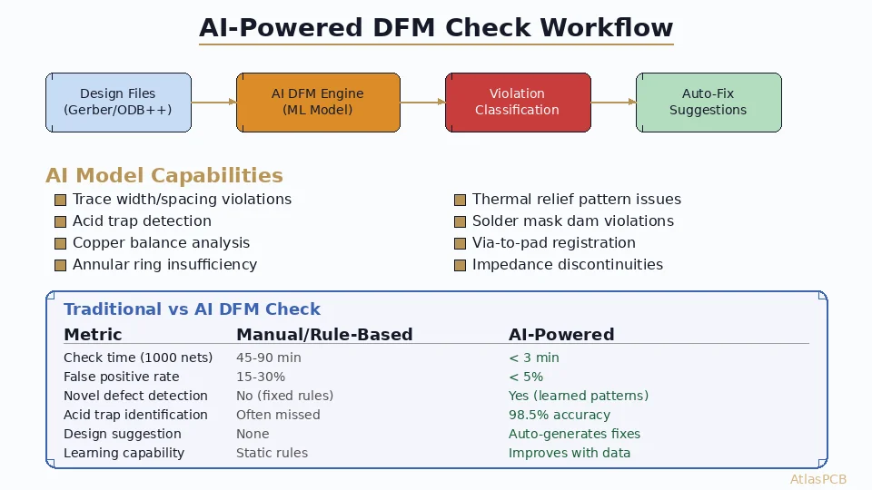
Request a DFM report with your first order. A good manufacturer provides detailed feedback, not just pass/fail.
Evaluate response quality. Does the manufacturer ask intelligent technical questions about your design? Or do they accept everything without comment?
How Atlas PCB Handles DFM
Every order at Atlas PCB includes a 12-hour human engineering DFM review:
- Stackup validation — mapped to actual available materials
- Impedance simulation — field solver verification on actual stackup
- Via analysis — aspect ratio, fill requirements, sub-lamination compatibility
- Copper balance assessment — warpage prediction
- Documentation review — completeness check with clarification requests
- Factory-specific constraint check — actual equipment capabilities, not generic rules
If issues are found, you receive a detailed report with the problem, impact, and proposed solution. No changes are made without your approval.
This review is included with every order — from 1-piece prototypes to production runs. Upload your Gerbers to get started.
Frequently Asked Questions
What does DFM check that DRC does not?
DRC checks geometric rules automatically — trace width, spacing, drill size, annular ring against predefined minimums. DFM is a human engineering assessment that evaluates your design against the real manufacturing process: whether the stackup can be built with available materials, whether your impedance targets work on the actual dielectric, whether vias will survive thermal cycling at the specified aspect ratio, and whether copper distribution will cause warpage. DFM catches problems that are invisible to software because they depend on manufacturing context.
Who is responsible for DFM — the designer or the manufacturer?
Both parties share responsibility. The designer should design within known manufacturing constraints, use appropriate design rules, and provide complete documentation. The manufacturer should review the design against their specific capabilities and alert the designer to issues before production. The most reliable outcomes come from collaboration — designer sends preliminary stackup to manufacturer before layout, manufacturer provides feedback, designer incorporates it. For complex boards, this collaboration is not optional.
How much does poor DFM cost?
A typical DFM-related respin costs $2,000-$20,000 including prototype reorder, manufacturing time, and engineering debug hours. In production, a DFM-caused yield problem can cost $50,000+ per lot in scrap, rework, and delays. Field failures traced to DFM issues (via cracking, impedance out of spec, delamination) can cost $100,000+ in warranty, investigation, and redesign. A DFM review takes hours and costs effectively nothing — it is the highest-ROI step in the PCB development process.
Related guides: [PCB DFM Checklist]/blog/pcb-dfm-checklist/) | [PCB Manufacturer with Engineering Review]/blog/pcb-manufacturer-engineering-review/) | [PCB Design Rules]/blog/pcb-design-rules-trace-width-spacing/)
Further Reading
[HDI PCB Design Guide: Stackup Rules, Via Structures & DFM Checklist]/blog/hdi-pcb-design-guide/)
[HDI PCB Technology: Microvias, Laser Drilling, and High-Density Design]/blog/hdi-pcb-technology/)
[PCB Sequential Lamination: Process, Design Rules, and When You Need It]/blog/pcb-sequential-lamination/)
[Via-in-Pad Design: Filled, Capped, and Plated Over — Complete Guide]/blog/via-in-pad-design/)
[Blind Via vs Buried Via: Design Rules, Cost Impact & When to Use Each]/blog/blind-via-vs-buried-via/)
[Controlled Impedance PCB: Design, Stackup & Testing Explained]/blog/controlled-impedance-pcb/)
[High-Multilayer FR4 vs Standard FR4: When to Upgrade Material Grade]/blog/high-multilayer-fr4-vs-standard-fr4/)
[PCB Manufacturing Process: 15 Steps from Gerber to Finished Board]/blog/pcb-manufacturing-process-15-steps/)
[ENEPIG vs ENIG: Which PCB Surface Finish for Your Design?]/blog/enepig-vs-enig/)
[PCB Surface Finish Guide: HASL, ENIG, OSP and More Compared]/blog/pcb-surface-finish-guide/)
About AtlasPCB — We specialize in complex PCB manufacturing for HDI, RF, and high-reliability applications. Explore our free engineering DFM review . Every order includes free engineering review. Get your quote.
Reviewed by AtlasPCB Engineering Team — IPC-certified manufacturing specialists with 15+ years of production experience in HDI, RF, and high-reliability PCB fabrication. Content based on factory floor data and real customer design reviews.
Frequently Asked Questions
What does DFM check that DRC does not?
Who is responsible for DFM — the designer or the manufacturer?
How much does poor DFM cost?
- DFM
- design for manufacturing
- pcb design
- manufacturing