· AtlasPCB Engineering Team · Engineering · 9 min read
Ultra-Thin PCB Manufacturing: Challenges, Design Rules, and Material Selection for Boards Under 0.4mm
A comprehensive guide to ultra-thin PCB manufacturing covering material selection, handling challenges, stackup constraints, and DFM rules for boards thinner than 0.4mm used in mobile devices, wearables, and IoT products.
Why Ultra-Thin PCBs Matter in Modern Electronics
The relentless drive toward smaller, lighter electronic devices has pushed PCB thickness below what was considered feasible just a decade ago. Smartphones now routinely incorporate motherboards thinner than 0.6mm, smartwatches demand substrates under 0.3mm, and medical implants require flexible-rigid constructions barely 0.2mm thick in their thinnest sections. This isn’t simply a matter of using thinner materials — ultra-thin PCB manufacturing demands fundamentally different process controls, handling methods, and design philosophies compared to standard-thickness boards.
At AtlasPCB, we define “ultra-thin” as any rigid or rigid-flex PCB with a finished thickness of 0.4mm (16 mil) or less. This threshold marks the point where conventional manufacturing assumptions break down: panels become fragile enough to crack during handling, registration tolerances tighten dramatically, and thermal processes must be carefully re-profiled to prevent warpage that would render the board unusable.
Material Selection for Ultra-Thin Constructions
Choosing the right laminate system is the single most critical decision in ultra-thin PCB design. The material must provide adequate mechanical strength at reduced thickness while maintaining consistent dielectric properties and surviving multiple thermal excursions during assembly.
Standard FR-4 remains viable down to approximately 0.3mm total thickness for 2-4 layer constructions, but designers must specify high-Tg variants (Tg ≥ 170°C) to prevent excessive Z-axis expansion during reflow. The glass weave style becomes critical at these thicknesses — 1080 and 2116 prepregs are too thick for most ultra-thin stackups, requiring 1035 or 106 glass styles that provide resin-rich constructions with thinner finished dielectric layers.
Low-CTE laminates from manufacturers like Mitsubishi (BT resin systems) and Panasonic (Megtron series) offer superior dimensional stability during thermal cycling. Their lower Z-axis CTE (typically 30-45 ppm/°C versus 50-70 ppm/°C for standard FR-4) significantly reduces the risk of via cracking in boards that lack the mechanical bulk to absorb thermal stress.
Polyimide-based materials dominate ultra-thin applications below 0.2mm, either as pure flex circuits or in rigid-flex configurations where the thin sections serve as interconnects between thicker rigid areas. DuPont’s Kapton and similar films maintain excellent dimensional stability at 25-50μm thickness, though they require specialized adhesive systems or adhesiveless bonding for reliable lamination.
Manufacturing Challenges Below 0.4mm
The manufacturing challenges multiply exponentially as thickness decreases. Understanding these constraints allows designers to make informed trade-offs between thinness, reliability, and cost.
Panel handling represents the most immediate practical challenge. A 0.3mm thick FR-4 panel measuring 18×24 inches deflects visibly under its own weight and can crack if handled with standard vacuum lifters. Manufacturers must invest in specialized thin-panel carriers — typically aluminum or stainless steel frames with vacuum or adhesive bonding — that support the panel throughout drilling, plating, imaging, and etching. These carriers add cost (typically 15-25% premium) and limit batch sizes, but they’re non-negotiable for consistent yield.
Drilling precision demands tighter control because the drill must penetrate a much thinner stackup without damaging the entry or exit surfaces. Drill aspect ratios that seem conservative for standard boards become aggressive in thin constructions — a 0.15mm drill through a 0.3mm board produces a 2:1 aspect ratio, which while not extreme in absolute terms, leaves almost no margin for drill wander or burr formation. Laser drilling becomes preferred for microvias, as mechanical drilling risks panel flexure during the process.
Lamination uniformity is far more difficult to achieve when the total stackup is thin. Pressure distribution across the lamination press must be nearly perfect — any variation creates thickness non-uniformity that translates directly into impedance variation. For controlled-impedance ultra-thin boards, manufacturers must document and control thickness tolerance to ±10% of the dielectric layer thickness, which at 50μm means ±5μm — approaching the resolution limits of standard measurement equipment.
Warpage control becomes the dominant yield limiter. IPC-6012 allows 0.75% bow and twist for standard boards, but even this relatively tight specification translates to only 0.15mm of bow across a 200mm board at 0.2mm thickness. In practice, achieving this requires symmetric stackups, balanced copper distribution, and carefully controlled cool-down profiles after lamination and solder mask cure. Asymmetric designs are essentially impossible to manufacture flat at these thicknesses.
Design Rules for Ultra-Thin PCBs
Designers accustomed to working with standard 1.6mm boards must adjust their approach significantly when targeting ultra-thin constructions.
Minimum trace width and spacing don’t change dramatically based on board thickness alone, but the available routing layers are severely constrained. A 0.3mm 4-layer stackup might offer only 50μm of dielectric between signal and reference planes, which actually benefits impedance by allowing narrower traces for a given impedance target — but the reduced dielectric thickness also increases crosstalk between adjacent traces on the same layer.
Via structures require careful consideration. Through-hole vias in a 0.3mm board have minimal barrel length, which can complicate reliable plating. The electroless copper seed layer and subsequent electroplating must achieve adequate thickness (minimum 20μm per IPC Class 2) in a very short via barrel, where solution exchange during plating is limited. Designers should prefer microvias where possible, as laser-drilled vias in thin dielectrics are well-characterized and highly reliable.
Copper weight selection directly impacts achievable board thickness. Starting with 1oz (35μm) copper on a thin core leaves minimal dielectric thickness between layers. Most ultra-thin designs use ½oz (18μm) or even ⅓oz (12μm) copper, accepting slightly higher resistance and reduced current capacity in exchange for thinner overall construction. For power delivery in thin boards, designers must rely on wider traces rather than heavier copper.
Panel utilization and breakaway tabs need special attention. Thin panels cannot support the same tab configurations used for standard boards — V-score is generally not recommended below 0.4mm total thickness because the score depth would penetrate too far into the board structure. Routed tabs with perforated break-away bridges are preferred, designed wide enough to prevent cracking during depaneling but narrow enough that the break occurs cleanly.
Stackup Examples for Common Thicknesses
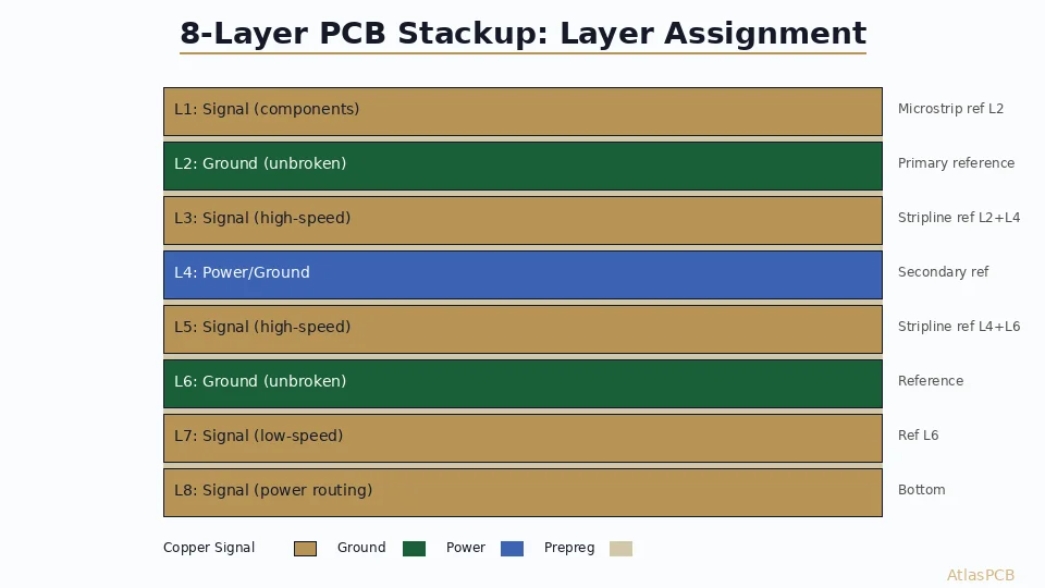
A practical 4-layer ultra-thin stackup at 0.3mm finished thickness might look like this:
The top copper layer uses ½oz (18μm) finished thickness, sitting on a 50μm prepreg layer (1035 glass, 70% resin content) over the first inner layer at ½oz. The core material is a 75μm laminate (also 1035 glass) with the second inner layer at ½oz on the bottom side, followed by another 50μm prepreg and the bottom copper layer at ½oz. After processing with solder mask on both sides (approximately 15μm each), the total comes to roughly 0.30mm.
This construction allows controlled impedance routing with approximately 50Ω single-ended on outer layers and 100Ω differential, though the margins are tight. Any manufacturing variation in dielectric thickness translates to proportionally larger impedance shifts than in a thicker board — reinforcing the need for test coupons on every production panel.
For 2-layer constructions at 0.2mm, designers typically use a single thin core (100-150μm) with ½oz copper on both sides. These boards are limited to simpler routing without internal reference planes, making them suitable for low-frequency digital or power distribution applications but inappropriate for high-speed signals requiring impedance control.
Reliability Considerations
Ultra-thin PCBs face unique reliability challenges that designers must address during the design phase rather than hoping manufacturing will solve them.
Thermal cycling creates proportionally more stress in thin boards because the reduced board stiffness allows greater Z-axis displacement during temperature excursions. Plated through-holes and microvias experience strain concentration at the knee (the junction between the via barrel and the pad), and in thin boards this strain cannot be distributed across a long barrel. Specifying via fill (either conductive or non-conductive epoxy) significantly improves reliability by preventing solder wicking into the short vias during assembly.
Mechanical shock and vibration resistance decreases with thickness by a cubic relationship — halving board thickness reduces bending stiffness by a factor of eight. Products using ultra-thin PCBs must either provide external mechanical support (stiffeners, enclosure features, or potting) or accept that the board will flex during use and design for that flex with appropriate trace routing angles and via placement away from high-stress areas.
Assembly compatibility requires close coordination between PCB fabrication and PCBA assembly teams. Ultra-thin boards may not be compatible with standard wave soldering fixtures, and even reflow profiles need adjustment because the reduced thermal mass means boards heat up faster and temperature uniformity is harder to maintain. Most ultra-thin assemblies use reflow-only processes with careful attention to panel support during the solder reflow profile.
Cost Factors and How to Optimize
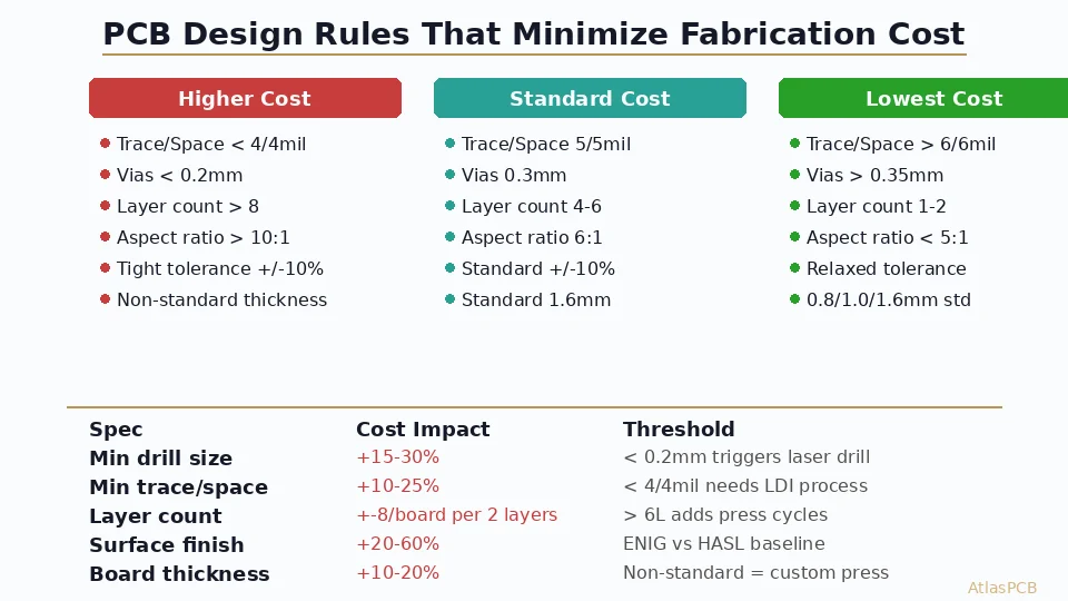
Ultra-thin PCB manufacturing costs 30-60% more than equivalent-complexity boards at standard thickness, driven primarily by carrier costs, reduced panel yield, and slower processing speeds. Several strategies can help manage costs without compromising quality.
First, design the stackup symmetrically wherever possible. Asymmetric constructions require special handling during lamination to counteract warpage, and any post-lamination flattening step risks damaging the thin panel. A symmetric design reduces both manufacturing complexity and reject rates.
Second, minimize the number of different drill sizes. Each drill change requires re-qualifying the drill parameters for the thin panel, and mechanical drilling on carriers requires different feeds and speeds than free-standing panels. Consolidating to fewer drill sizes reduces setup time and improves consistency.
Third, consider rigid-flex construction if only portions of the design require ultra-thin thickness. A rigid-flex approach allows standard-thickness rigid sections (simpler and cheaper to manufacture) connected by thin flex sections where space constraints demand it. The overall assembly may cost less than an entirely ultra-thin rigid board while offering better reliability in the thicker sections.
When to Choose Ultra-Thin PCBs
Not every space-constrained design requires ultra-thin construction. Before committing to a sub-0.4mm design, engineers should evaluate whether alternative approaches — such as HDI with higher layer counts, chip-on-board assembly, or package-on-package stacking — might achieve the same form factor goals with less manufacturing risk.
Ultra-thin PCBs make the most sense when the application genuinely requires a uniformly thin, rigid substrate: smartphone motherboards, smart card modules, certain medical implants, and ultra-compact IoT sensors. For applications where thickness constraints are localized rather than uniform, rigid-flex or selective milling (creating thin areas within a standard-thickness board) often provides a better cost-reliability balance.
At AtlasPCB, we regularly manufacture boards down to 0.2mm thickness in production volumes, with prototype capabilities to 0.15mm for evaluation builds. Early engagement with our engineering team during the design phase allows us to recommend optimal material systems, identify potential manufacturing risks, and provide DFM feedback before the design is finalized — saving both time and cost in the development cycle.
About AtlasPCB — We specialize in complex PCB manufacturing for HDI, RF, and high-reliability applications. Explore our HDI PCB manufacturing capabilities, or get an free engineering DFM review . Every order includes free engineering review. Get your quote.
Reviewed by AtlasPCB Engineering Team — IPC-certified manufacturing specialists with 15+ years of production experience in HDI, RF, and high-reliability PCB fabrication. Content based on factory floor data and real customer design reviews.
- ultra-thin-pcb
- pcb-manufacturing
- thin-board
- hdi
- wearables
- mobile-pcb
- dfm