· Sophia Reyes · Engineering · 4 min read
Single-Layer vs Multi-Layer PCB
Compare single-layer, double-layer, and multi-layer PCBs — understand the differences in cost, complexity, performance, and applications to choose the right layer count for your project.

Quick Answer
Single-layer PCBs have copper on one side only (simplest, cheapest), double-layer on both sides with through-hole vias, and multilayer PCBs (4-30+ layers) sandwich inner copper layers between dielectric. Layer count increases with design complexity, signal speed, and component density.
One of the most fundamental decisions in PCB design is choosing the number of layers. The layer count affects cost, routing complexity, signal integrity, board size, and manufacturing lead time. This guide compares different layer configurations to help you make the right choice.
Understanding PCB Layers
Each “layer” in a PCB refers to a sheet of copper that carries electrical traces. The layers are separated by insulating dielectric material (typically FR-4 prepreg or core). A 4-layer PCB, for example, has four separate copper layers sandwiched together.
Single-Layer PCB (1-Layer)
Structure
One copper layer on one side of the substrate, with solder mask and silkscreen.
Characteristics
- Simplest design: Components and traces on one side only
- Lowest cost: Minimal material and processing steps
- No vias needed: All routing on a single plane
- Limited routing density: Complex circuits impossible
Typical Applications
- LED lighting strips
- Simple power supplies
- Calculator circuits
- Radio/AM receivers
- Relay control boards
- Toy electronics
Cost Benchmark
~$0.10-0.30 per board (100x100mm, qty 100)
Double-Layer PCB (2-Layer)
Structure
Copper on both sides of the substrate, connected by plated through-hole vias.
Characteristics
- Doubled routing area: Components and traces on both sides
- Through-hole vias connect top and bottom layers
- Moderate cost: Only marginally more expensive than single-layer
- Good for most applications: Handles moderate complexity circuits
Typical Applications
- IoT devices and sensor modules
- LED drivers
- Industrial control boards
- Power converters
- Audio amplifiers
- Arduino/Raspberry Pi shields
Cost Benchmark
~$0.20-0.60 per board (100x100mm, qty 100)
4-Layer PCB
Structure
Four copper layers: typically Signal-Ground-Power-Signal, with three dielectric layers.
Characteristics
- Dedicated ground and power planes: Dramatically improves signal integrity and EMI performance
- Better impedance control: Consistent reference planes for controlled impedance traces
- Higher routing density: Two routing layers plus two plane layers
- Reduced EMI: Solid ground plane acts as a shield
Typical Applications
- USB, HDMI, and Ethernet interfaces
- Microcontroller-based systems
- Bluetooth/Wi-Fi modules
- Industrial automation
- Medical monitoring devices
- Automotive ECUs
Cost Benchmark
~$0.80-2.00 per board (100x100mm, qty 100)

6-Layer PCB
Structure
Six copper layers, often: Signal-Ground-Signal-Signal-Power-Signal
Characteristics
- Three routing layers plus dedicated ground and power planes
- Excellent signal integrity for high-speed designs
- Better thermal management with additional copper planes
- Compact designs possible for complex circuits
Typical Applications
- High-speed digital designs (DDR3/DDR4 memory interfaces)
- FPGA-based systems
- Network switches and routers
- GPS receivers
- Advanced medical equipment
Cost Benchmark
~$2.00-5.00 per board (100x100mm, qty 100)
8-Layer and Beyond
8-Layer
Commonly used for: DDR4/DDR5 memory, PCIe Gen3/Gen4, gigabit Ethernet
10-12 Layer
Server motherboards, advanced networking equipment, high-performance computing
14-20+ Layer
Supercomputers, high-density FPGA boards, aerospace avionics, 5G base station equipment
Cost Scaling
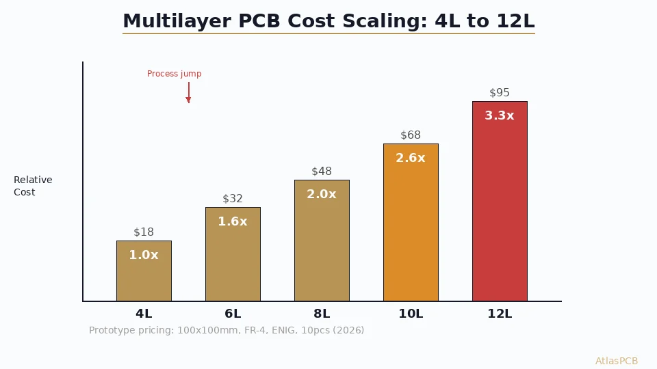
Each additional layer pair adds roughly 30-40% to the base cost.
Comparison Table
| Feature | 1-Layer | 2-Layer | 4-Layer | 6-Layer | 8-Layer |
|---|---|---|---|---|---|
| Cost | Lowest | Low | Medium | Medium-High | High |
| Routing density | Very low | Low-Medium | Medium-High | High | Very High |
| Signal integrity | Poor | Fair | Good | Very Good | Excellent |
| EMI performance | Poor | Fair | Good | Very Good | Excellent |
| Impedance control | No | Limited | Good | Very Good | Excellent |
| Thermal performance | Poor | Fair | Good | Good | Very Good |
| Max frequency | <10 MHz | <100 MHz | <1 GHz | <3 GHz | <10+ GHz |
| Lead time | 1-2 days | 2-3 days | 3-5 days | 5-7 days | 7-10 days |
How to Choose the Right Layer Count
Choose 1-2 Layers When:
- Circuit complexity is low (fewer than 50 components)
- Maximum operating frequency is below 50 MHz
- Cost is the primary concern
- Board size is not constrained
- No controlled impedance requirements
Choose 4 Layers When:
- You need a solid ground plane for signal integrity
- Operating frequency exceeds 50 MHz
- USB, SPI, I2C, or UART at moderate speeds
- Mixed analog and digital circuits
- EMC compliance is required
Choose 6+ Layers When:
- High-speed digital interfaces (DDR, PCIe, USB 3.0+)
- Multiple power domains requiring separate planes
- RF/microwave circuits requiring stripline routing
- Dense BGA packages with many I/O pins
- Strict EMI requirements (medical, automotive)
Cost Optimization Tips
- Route on fewer layers: Just because you have 4 layers doesn’t mean you must use all for routing. Use 2 for signals and 2 for planes.
- Increase board size before adding layers: Sometimes a slightly larger 2-layer board is cheaper than a compact 4-layer one.
- Standard stackups: Use your manufacturer’s standard stackups to avoid custom lamination charges.
- Panelization: Combine multiple designs on one panel to reduce per-board cost.
- Standard thickness: 1.6mm is the most cost-effective board thickness for most layer counts.
Conclusion
The right layer count balances performance requirements with cost and manufacturability. For most general electronics, a 2-layer or 4-layer PCB handles the job well. As signal speeds increase and designs become more complex, moving to 6 or more layers provides the signal integrity and routing density needed for reliable high-performance products.
Further Reading
[Controlled Impedance PCB: Design, Stackup & Testing Explained]/blog/controlled-impedance-pcb/)
[High-Speed PCB Design: Signal Integrity Essentials for Modern Electronics]/blog/high-speed-pcb-design/)
[PCB Stackup Design: Best Practices for Signal Integrity and EMI Control]/blog/pcb-stackup-design-guide/)
[PCB Solder Mask: Types, Colors, and Functions Explained]/blog/pcb-solder-mask-guide/)
[PCB Thermal Management: Heat Dissipation Techniques for Reliable Electronics]/blog/pcb-thermal-management/)
[HDI PCB Design Guide: Stackup Rules, Via Structures & DFM Checklist]/blog/hdi-pcb-design-guide/)
[Multilayer PCB Stackup Design Guide: 8 to 30+ Layers Step by Step]/blog/multilayer-pcb-stackup-design-guide/)
[EMC/EMI Design for PCBs: Passing Compliance on the First Try]/blog/emc-emi-pcb-design/)
[PCB Grounding Techniques: Star, Split, and Solid Ground Plane Strategies]/blog/pcb-grounding-techniques/)
[PCB Cost Optimization: 15 Practical Ways to Reduce Board Cost]/blog/pcb-cost-optimization/)
About AtlasPCB — We specialize in complex PCB manufacturing for HDI, RF, and high-reliability applications. Explore our multilayer PCB fabrication up to 30 layers . Every order includes free engineering review. Get your quote.
Reviewed by AtlasPCB Engineering Team — IPC-certified manufacturing specialists with 15+ years of production experience in HDI, RF, and high-reliability PCB fabrication. Content based on factory floor data and real customer design reviews.
Frequently Asked Questions
When do I need a multilayer PCB?
How much more does a 4-layer PCB cost vs 2-layer?
- multilayer pcb
- pcb design
- layer stackup