· Marcus Lin · Engineering · 6 min read
RF Via Stitching and Ground Plane Isolation
Learn how via stitching creates effective Faraday cage isolation for RF signals, preventing parallel-plate waveguide modes and cavity resonance in PCB designs above 6 GHz.
Quick Answer
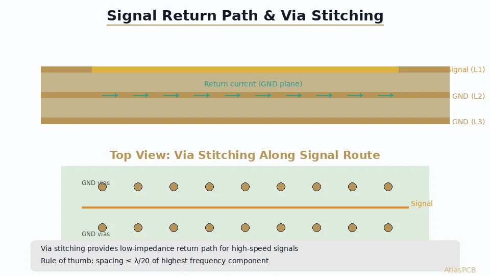
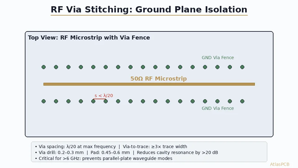
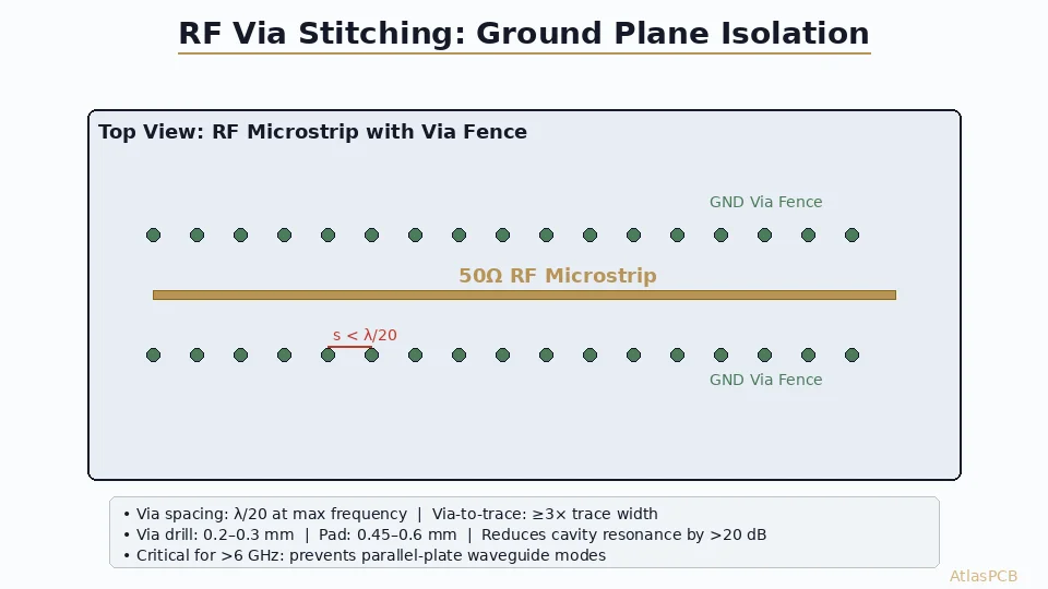
RF via stitching creates a Faraday cage by placing ground vias at intervals of λ/20 or less alongside signal traces, preventing electromagnetic field leakage between ground planes and suppressing parallel-plate waveguide modes that cause cavity resonance above 6 GHz.
Why Via Stitching Matters for RF PCB Performance
As wireless systems push beyond 6 GHz — spanning 5G mmWave, automotive radar (77 GHz), satellite communications, and Wi-Fi 7 — the PCB substrate itself becomes an electromagnetic structure. The parallel ground planes in a multilayer board form a cavity that can resonate at frequencies where the plane dimensions equal half-wavelength multiples.
Without proper via stitching, these cavity resonances create unpredictable impedance variations, crosstalk pathways, and radiation leakage that degrade RF performance by 10-20 dB in worst-case scenarios.
The Physics: Parallel-Plate Waveguide Modes
A pair of ground planes separated by a dielectric forms a parallel-plate waveguide. The resonant frequency of a rectangular cavity is given by:
f_resonant = (c / 2√εr) × √((m/a)² + (n/b)²)
Where:
- c = speed of light (3×10⁸ m/s)
- εr = dielectric constant
- a, b = plane dimensions
- m, n = mode indices
For a 50 mm × 50 mm board area with FR-4 (εr = 4.2), the first resonant mode (TM₁₀) occurs at approximately 1.46 GHz. By 10 GHz, dozens of modes are excited simultaneously.
Impact on Signal Integrity
When a signal trace crosses a resonant cavity, the return path current encounters high impedance at resonance, causing:
- Impedance discontinuities — localized Z₀ variations of ±15-30%
- Radiation leakage — energy couples out through board edges
- Crosstalk amplification — cavity modes create coupling paths between unrelated traces
- Return loss degradation — S11 can spike above -10 dB at resonant frequencies
Via Stitching Design Rules
Spacing Formula
The fundamental rule: via spacing must be less than λ/20 at the highest frequency of interest.
| Frequency | λ in FR-4 (εr=4.2) | Max Via Spacing (λ/20) |
|---|---|---|
| 6 GHz | 24.4 mm | 1.22 mm |
| 10 GHz | 14.6 mm | 0.73 mm |
| 24 GHz | 6.1 mm | 0.30 mm |
| 28 GHz | 5.2 mm | 0.26 mm |
| 77 GHz | 1.9 mm | 0.095 mm |
For 77 GHz automotive radar, via spacing requirements approach the limits of mechanical drilling. Laser-drilled microvias (75-100 μm) become mandatory.
Via Geometry Selection
The via itself must present low impedance at the operating frequency:
- Drill diameter: 0.2-0.3 mm (standard) or 0.075-0.1 mm (microvia for >30 GHz)
- Pad diameter: Drill + 0.25 mm minimum annular ring
- Anti-pad: Keep anti-pad minimal (0.5 mm typical) to maximize copper plane continuity
- Aspect ratio: ≤8:1 for reliable plating; ≤1:1 for microvias
Via-to-Trace Clearance
The ground via fence must maintain adequate clearance from the signal trace to avoid impedance perturbation:
- Minimum clearance: 3× trace width
- Recommended: 4-5× trace width for sensitive 50 Ω lines
- Maximum: Keep within 2× substrate thickness to maintain shielding effectiveness
Need RF PCB Manufacturing with Tight Via Tolerances?
AtlasPCB specializes in high-frequency boards with ±0.05 mm via placement accuracy, laser-drilled microvias, and Rogers/PTFE material processing.
Get an RF PCB Quote →Via Fencing for Trace Isolation
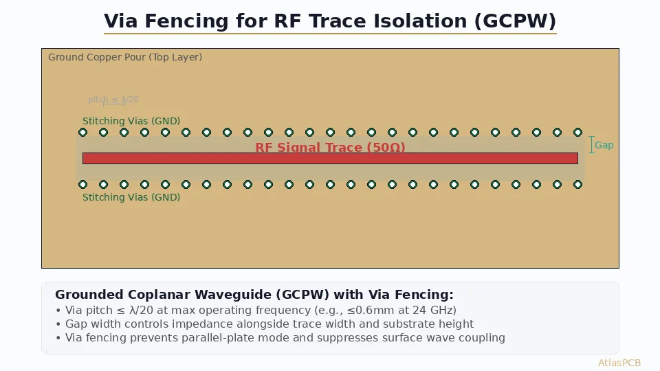
While via stitching addresses area-wide cavity suppression, via fencing creates a localized Faraday cage around individual RF traces or sensitive circuits.
Single-Row Fence Design
A single row of ground vias parallel to a signal trace provides approximately 20-30 dB of isolation below the first fence resonance frequency.
Key parameters:
- Via pitch along the fence: λ/20 maximum
- Distance from trace center: 3-5× trace width
- Via connection: Must connect all ground layers (not just adjacent)
Double-Row Fence (Enhanced Isolation)
For isolation requirements exceeding 40 dB (common in duplexer and filter sections), implement a double row:
- Offset second row by half the pitch (staggered arrangement)
- Achieves 40-60 dB isolation when properly implemented
- Required for TX/RX isolation in integrated front-end modules
Fence Termination
At the ends of via fences, EMI can leak around corners. Best practices:
- Wrap corners — Continue the via fence around 90° bends
- Extra vias at transitions — Add 2-3 additional vias where traces change direction
- Close the cage — Connect fence rows at both ends to form a complete enclosure
Implementation in Multilayer Stackups
4-Layer RF Board
For a typical 4-layer RF stackup (Signal-Ground-Ground-Signal):
- Stitch between L2 and L3 ground planes every 1-2 mm (for 10 GHz)
- Fence critical RF traces on L1 with vias connecting L2-L3-L4
- Ensure no splits in ground planes under RF routing
6+ Layer RF Board
For complex multilayer boards with multiple RF sections:
- Dedicated RF ground: Assign one plane layer exclusively for RF return current
- Cage construction: Create complete via cages around individual RF blocks
- Compartmentalization: Use via walls to divide the board into isolated RF zones (LNA, PA, mixer, LO)
Common Mistakes and How to Avoid Them
Mistake 1: Insufficient Via Density at High Frequencies
Problem: Using 2 mm via spacing for a 28 GHz design (requires 0.26 mm).
Solution: Always calculate spacing based on highest harmonic, not just fundamental. For a 28 GHz fundamental, consider up to the 3rd harmonic (84 GHz) for via stitching near non-linear components.
Mistake 2: Via Stubs Creating Resonance
Problem: Through-hole vias on inner-layer RF traces leave stubs that resonate at quarter-wavelength frequencies.
Solution: Use back-drilling to remove stubs, or use blind/buried vias. A 1 mm stub resonates at approximately 37 GHz in FR-4.
Mistake 3: Ground Plane Splits Under Via Fences
Problem: A gap in the reference plane under a via fence creates a slot antenna.
Solution: Ensure continuous ground copper under and around all via fences. Never route power traces or other signals that require plane splits in RF areas.
Mistake 4: Mixing Signal and Stitching Vias
Problem: Using the same via pattern for both signal transitions and ground stitching, creating confusion in manufacturing and increasing cost.
Solution: Clearly distinguish stitching vias in your design rules. Use a specific padstack (e.g., 0.25 mm drill, no-connect net assignment to GND) for all stitching vias.
Manufacturing Considerations
Drill Limitations
| Feature | Standard Mechanical | Laser (HDI) |
|---|---|---|
| Min drill | 0.2 mm | 0.075 mm |
| Positional accuracy | ±0.05 mm | ±0.025 mm |
| Aspect ratio | 8:1 | 1:1 |
| Cost impact | Baseline | +30-60% |
| Max frequency suitability | ~20 GHz | 77+ GHz |
Cost Optimization Strategies
- Prioritize fencing near traces — Only place dense stitching where cavity modes would impact signal paths
- Use different pitches for different zones — Dense in RF areas, relaxed in digital sections
- Combine with copper fill — Stitched copper pours are more effective than isolated via arrays
- Minimize unique drill sizes — Standardize stitching via geometry to reduce drill changes
Simulation and Verification
Pre-Layout Analysis
Before routing, perform a cavity resonance simulation:
- Define board outline and layer stackup in a 3D EM solver (HFSS, CST)
- Identify resonant modes within the operating bandwidth
- Place via stitching to shift or suppress problematic modes
- Verify with S-parameter extraction
Post-Layout Verification
After placement and routing:
- Extract the power/ground plane impedance profile (Z11 of the cavity)
- Check for impedance peaks within ±20% of operating frequency
- Verify isolation between RF compartments using coupling simulations
- Validate via fence effectiveness with near-field radiation plots
Further Reading
- Controlled Impedance PCB Design and Stackup Calculations
- PCB Hybrid Stackup: Rogers + FR-4 Integration
- Differential Impedance for PCIe Gen5 and DDR5
Ready to Manufacture Your RF PCB?
Designing high-frequency boards with aggressive via stitching requirements? AtlasPCB offers laser-drilled microvias down to 75 μm, ±0.025 mm positional accuracy, and extensive experience with Rogers, Taconic, and PTFE substrates for frequencies up to 77 GHz.
About AtlasPCB — We specialize in complex PCB manufacturing for HDI, RF, and high-reliability applications. Explore our RF and high-frequency PCB services, or get an impedance-controlled PCB manufacturing . Every order includes free engineering review. Get your quote.
Reviewed by AtlasPCB Engineering Team — IPC-certified manufacturing specialists with 15+ years of production experience in HDI, RF, and high-reliability PCB fabrication. Content based on factory floor data and real customer design reviews.
Frequently Asked Questions
What is the optimal via spacing for RF via stitching?
When does via stitching become necessary in PCB design?
How does via stitching differ from via fencing?
- rf pcb
- via stitching
- ground plane
- cavity resonance
- high frequency
- microwave
- signal integrity