· AtlasPCB Engineering · Engineering · 11 min read
RF PCB Design and Manufacturing: Complete Workflow from Simulation to Fab-Ready Output Package
A step-by-step engineering guide covering the complete RF PCB workflow — from electromagnetic simulation constraints through layout, DFM verification, and the fabrication output package your manufacturer needs to build Rogers and PTFE boards correctly the first time.
Quick Answer
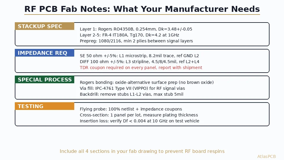
A complete RF PCB output package requires four elements beyond standard Gerbers: a detailed stackup specification with exact material callouts (manufacturer part numbers, not generic names), impedance control table with trace geometries and reference planes, special process notes (Rogers bonding method, via fill type, backdrill depth), and testing requirements (TDR targets, insertion loss limits). Missing any one of these causes delays or fabrication errors on Rogers and PTFE boards.
Quick Reference: RF PCB Output Package Completeness Checklist
| Document | What It Must Contain | Consequence If Missing |
|---|---|---|
| Stackup drawing | Material part numbers, thicknesses, copper weights | Wrong dielectric = impedance failure |
| Impedance table | Targets, tolerances, trace widths, reference planes | Manufacturer guesses or uses wrong refs |
| Special process notes | Rogers bonding, via fill type, backdrill specs | Wrong process = delamination or signal loss |
| Test requirements | TDR targets, coupon design, acceptance criteria | No verification = ship-and-hope approach |
| Material equivalence list | Acceptable alternatives with Dk/Df ranges | Delays when specified material is unavailable |
If you deliver only Gerbers and a drill file for an RF board, you are leaving critical manufacturing decisions to someone who has never seen your simulation. This article walks through exactly what your output package needs to contain and why each element matters for first-pass success.
Step 1: From Simulation to Stackup Specification
The RF PCB design workflow starts with electromagnetic simulation — typically in HFSS, CST, or Ansys SIwave — where you define transmission line geometries that achieve your target impedance and loss budget. The critical transition happens when you convert those simulation parameters into a fabrication stackup that a manufacturer can actually build.
The most dangerous assumption engineers make is that the material properties in their simulator exactly match what ends up in the manufactured board. In reality, every PCB laminate has Dk variation across production lots, and the Dk values published in datasheets are measured under specific conditions (frequency, temperature, moisture content) that may differ from your operating environment. This is why your stackup specification must communicate intent, not just dimensions.
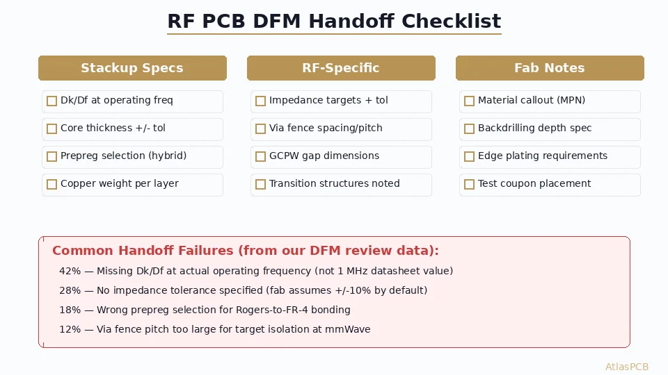
A proper stackup specification for RF boards includes the exact material manufacturer and product number (e.g., “Rogers RO4350B LoPro, 0.254mm nominal core thickness”), the copper foil type and weight (ED vs RTF matters for loss at high frequency), the design Dk value you used in simulation with the measurement frequency, and any constraints on prepreg selection for the non-RF layers. In our engineering reviews, approximately 1 in 4 RF board submissions contain a stackup specification generic enough to allow material substitutions that would shift impedance outside tolerance.
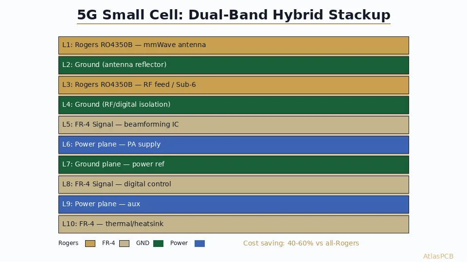
For hybrid stackups — the most common construction for mixed RF and digital boards — you need to specify which layers use Rogers or PTFE cores and which use standard FR-4, along with the bondply or prepreg material used between dissimilar materials. The bonding layer between Rogers and FR-4 has its own Dk and thickness that affects impedance on adjacent layers, and this is frequently omitted from stackup drawings. Our process engineers use specific bonding materials (typically Rogers 4450F or Taconic FastRise 27) whose properties we’ve characterized at production temperatures.
RF STACKUP EXPERTISE
Need Help Translating Simulation to Fabrication Stackup?
Our RF process engineers validate your stackup against actual material properties and manufacturing constraints before first article.
RF PCB Capabilities ›
Step 2: Impedance Control Specification
The impedance control table is arguably the most important document in your RF PCB output package. It bridges the gap between your design intent and the manufacturer’s fabrication reality by explicitly stating what impedance targets must be achieved and how they should be verified.
A proper impedance table contains: the target impedance value and tolerance (e.g., “50 ohm single-ended, +/-5%”), the physical trace geometry you’ve calculated (trace width, gap for differential, distance to reference plane), the specific reference plane layer, and any notes about which field solver model applies (microstrip, buried microstrip, edge-coupled stripline, etc.). This last point matters because different solver models produce different impedance predictions for the same geometry — a 10-15% discrepancy between microstrip and embedded microstrip models is common for the same physical cross-section.
From our production experience, the most impactful specification often overlooked is the measurement method. Stating ”+/-5% tolerance” is meaningless without specifying how compliance is verified. For RF boards, you should specify: “TDR measurement on dedicated test coupon, rise time corresponding to 10 GHz bandwidth, measured after solder mask application.” The solder mask thickness affects microstrip impedance by 2-4 ohms and must be included in the measurement baseline.
We’ve seen cases where engineers achieve beautiful simulation results at 50.0 ohms, specify +/-5% tolerance, and then the manufacturer’s TDR measurement on a bare board (pre-solder mask) shows 48.5 ohms — technically in spec. After solder mask application, the actual impedance drops to 46.2 ohms, now outside the +/-5% window. This happens because the test coupon was measured before mask, while the production board operates after mask. Specifying the measurement point prevents this disconnect.
For differential pairs, also specify the intra-pair skew tolerance and whether your impedance targets apply to the odd-mode impedance or the differential-mode impedance. These differ by a factor of 2 in the definition, and a miscommunication here means your 100-ohm differential pair gets built as a 50-ohm differential pair (100-ohm single-ended odd mode).
Step 3: Special Process Notes for Rogers and PTFE
Rogers and PTFE laminates require manufacturing processes that differ significantly from standard FR-4. If your fab notes don’t specify these processes, the manufacturer will apply standard FR-4 techniques — which can cause delamination, poor copper adhesion, and drilling defects on specialty materials.
The critical process differences that must be called out in your fabrication notes:
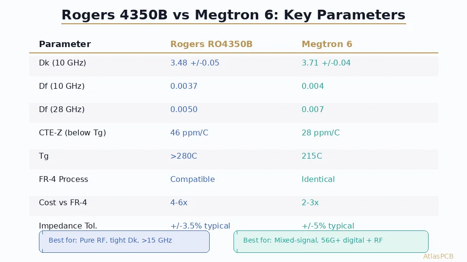
Surface preparation for bonding: Standard FR-4 uses brown oxide or black oxide treatment before lamination to promote copper-prepreg adhesion. Rogers 4350B specifically requires an alternative surface preparation — the manufacturer should use a micro-etch or silane-based treatment rather than oxide. If standard brown oxide is applied to Rogers copper, adhesion can be 30-50% lower than specification, creating a latent reliability risk that passes initial testing but fails under thermal cycling.
Drill parameters: Rogers and PTFE materials have different optimal drill speeds and feed rates compared to FR-4. PTFE materials in particular tend to smear during drilling if feed rates are too aggressive, creating a resin layer over the copper that prevents reliable plating. Your fab notes should state “drill with PTFE-appropriate parameters — reduced feed rate, sharp carbide bits, de-smear process required after drilling.” If the manufacturer doesn’t have documented PTFE drill recipes, they likely aren’t experienced with the material.
Via fill requirements: For RF boards requiring via-in-pad (common for BGA RF components and ground vias under GCPW traces), specify the via fill type per IPC-4761. Type VII (conductive fill with copper cap) provides the lowest insertion loss for ground stitching vias, but not all manufacturers can achieve reliable fill on 0.2mm vias in Rogers core material. Our process uses a specific conductive paste formulated for compatibility with Rogers thermal expansion characteristics, applied in a vacuum-assist screen printing process to eliminate voids.
Backdrill specifications: When your stackup includes through-hole vias that penetrate RF signal layers, backdrill (controlled-depth drilling from the back side) removes the via stub that causes resonance and impedance discontinuity. Your fab notes must specify: which vias require backdrill, the target stub length (typically 5-8 mils maximum), and the acceptable tolerance on drill depth (typically +/-3 mils). Our process uses X-ray measurement of actual copper position before backdrill to achieve consistent stub removal even when board thickness varies across the panel.
ROGERS SPECIALIZATION
Experienced with Rogers 4350B Hybrid Construction
Our facility runs Rogers and PTFE boards weekly with documented process recipes and characterized bonding parameters.
Submit RF Design ›Step 4: Testing and Acceptance Criteria
The final element of your RF PCB output package defines how the finished boards will be verified and what constitutes an acceptable delivery. Without explicit testing requirements, manufacturers default to their standard inspection protocol — which for most shops means netlist electrical test (continuity/isolation) and visual inspection. For RF boards, this is grossly insufficient.
Your testing specification should include three levels: standard production testing (netlist continuity + isolation), impedance verification (TDR on dedicated coupons), and — for critical applications — insertion loss or material property verification.
For the impedance coupons, specify the coupon design geometry that matches your production traces. The coupon should replicate the exact trace width, spacing, reference plane distance, and material stackup of your critical RF traces. If your board has multiple impedance zones (e.g., 50 ohm microstrip on Layer 1 and 100 ohm differential stripline on Layer 3), each zone needs a corresponding coupon. The coupon length should be sufficient for clean TDR measurement — typically 100-150mm of controlled-impedance trace with proper SMA launch transitions.
For boards operating above 10 GHz, TDR impedance alone may not guarantee adequate performance because it doesn’t capture frequency-dependent loss. In these cases, specify insertion loss measurement on a test trace at your operating frequency, with a maximum acceptable value derived from your link budget. This catches material quality issues (high Df from contaminated prepreg) and fabrication issues (rough copper surfaces from excessive micro-etch) that TDR alone misses.
Our standard RF board package includes: 100% netlist test, TDR impedance measurement on all specified coupon types (minimum 2 coupons per panel, one from each long edge), cross-section analysis on one panel per production lot (measuring actual plating thickness, dielectric thickness, and copper roughness), and photographic documentation of any Rogers handling or bonding anomalies. We provide all measurement data in a digital format that customers can import into their incoming inspection database.
COMPLETE VERIFICATION
TDR Reports Included with Every RF Board Order
Impedance verification on every production panel — no extra charge, no separate request needed.
Our Testing Capabilities ›Common Mistakes in RF PCB Output Packages
Based on the DFM reviews our engineering team performs daily, these are the most frequent issues we find in RF PCB fab packages that cause delays or failures:
The most common mistake is specifying “FR-4” generically for non-RF layers in a hybrid stackup. “FR-4” encompasses materials with Dk ranging from 3.8 to 4.8 and Df from 0.010 to 0.025. If your impedance simulation assumes Dk=4.2 for the FR-4 layers, but the manufacturer uses a high-Tg FR-4 with Dk=4.5, your impedance on those layers shifts by approximately 7%. Always specify the exact FR-4 grade (e.g., “Shengyi S1000-2M, Dk=4.2 +/-0.1 at 1 GHz”) or at minimum provide an acceptable Dk range.
The second most common issue is omitting copper roughness specifications. At frequencies above 5 GHz, copper surface roughness becomes a dominant loss mechanism. Standard electrodeposited (ED) copper has RMS roughness of 1.5-2.5 um, which increases insertion loss by 30-60% at 10 GHz compared to low-profile (RTF/HVLP) copper at 0.3-0.5 um RMS. If your simulation uses ideal conductors or low-roughness copper parameters, but the manufacturer uses standard ED foil, your measured insertion loss will exceed predictions. State the copper foil type explicitly: “HVLP grade copper, Rz less than 3 um” for boards above 5 GHz.
ATLASPCB
First RF Board Order? Let Us Review Your Package.
Upload your design and we identify specification gaps before they become manufacturing problems. Our RF team reviews every Rogers and PTFE design before production.
Get Engineering Review ›
Reviewed by AtlasPCB Engineering Team — 15+ years in advanced PCB fabrication for RF, HDI, and rigid-flex applications.
Related Reading:
About AtlasPCB — We specialize in complex PCB manufacturing for HDI, RF, and high-reliability applications. Explore our RF and high-frequency PCB services, Rogers RO4350B PCB manufacturing, or get an impedance-controlled PCB manufacturing . Every order includes free engineering review. Get your quote.
Reviewed by AtlasPCB Engineering Team — IPC-certified manufacturing specialists with 15+ years of production experience in HDI, RF, and high-reliability PCB fabrication. Content based on factory floor data and real customer design reviews.
Frequently Asked Questions
What fabrication files does an RF PCB manufacturer need beyond standard Gerbers?
Should I specify trace width or target impedance in my fab notes?
How do I specify Rogers material in a fabrication drawing?
What testing should I require for RF PCBs?
What is the most common reason RF PCBs fail in manufacturing?
- RF PCB design and manufacturing
- impedance controlled PCB manufacturer
- Rogers 4350B stackup
- PCB DFM check
- China RF PCB manufacturer