· Marcus Lin · Engineering · 4 min read
RF and Microwave PCB Design
Learn RF/microwave PCB design essentials — material selection, transmission line structures, grounding techniques, component placement, and manufacturing considerations for 1-40+ GHz circuits.

Quick Answer
RF and microwave PCB design requires specialized materials (Rogers, Taconic, PTFE), controlled impedance transmission lines, proper grounding techniques, and careful component placement. At frequencies from 1-40+ GHz, every trace acts as a transmission line and every via as an inductor.
RF and microwave PCB design operates in a realm where every trace is a transmission line, every via is an inductor, and every copper shape is a potential antenna. Designing for frequencies from 1 GHz to 40+ GHz requires specialized knowledge of materials, layout techniques, and manufacturing processes.
Frequency Bands and Applications
| Band | Frequency | Applications |
|---|---|---|
| L-band | 1-2 GHz | GPS, satellite phone, 4G LTE |
| S-band | 2-4 GHz | WiFi 2.4GHz, Bluetooth, radar |
| C-band | 4-8 GHz | WiFi 5/6GHz, 5G Sub-6, satellite |
| X-band | 8-12 GHz | Radar, satellite communications |
| Ku-band | 12-18 GHz | Satellite TV, radar |
| K/Ka-band | 18-40 GHz | 5G mmWave, automotive radar, satellite |
| V-band | 40-75 GHz | 60GHz WiGig, radar |
Material Selection for RF
FR-4 is acceptable up to ~2-3 GHz with careful design. Above that, specialized materials are needed.
Material Comparison for RF
| Material | Dk | Df (10GHz) | Dk Tolerance | Cost vs FR-4 | Max Freq |
|---|---|---|---|---|---|
| FR-4 | 4.2-4.8 | 0.020 | +/-10% | 1x | ~3 GHz |
| RO4003C | 3.38 | 0.0027 | +/-1.5% | 4x | ~20 GHz |
| RO4350B | 3.48 | 0.0037 | +/-1.5% | 4x | ~15 GHz |
| RO3003 | 3.00 | 0.0013 | +/-1.3% | 10x | ~40 GHz |
| RT5880 | 2.20 | 0.0009 | +/-0.9% | 15x | ~60 GHz |
Key Material Properties for RF
- Low Dk: Lower dielectric constant means wider traces for 50 ohm impedance (easier to manufacture) and less signal delay
- Low Df: Lower loss factor means less signal attenuation per unit length
- Tight Dk tolerance: Ensures consistent impedance across the board and batch-to-batch
- Dk stability vs frequency: Dk should remain constant across the operating bandwidth
- Dk stability vs temperature: Critical for outdoor and automotive applications
RF Transmission Line Structures
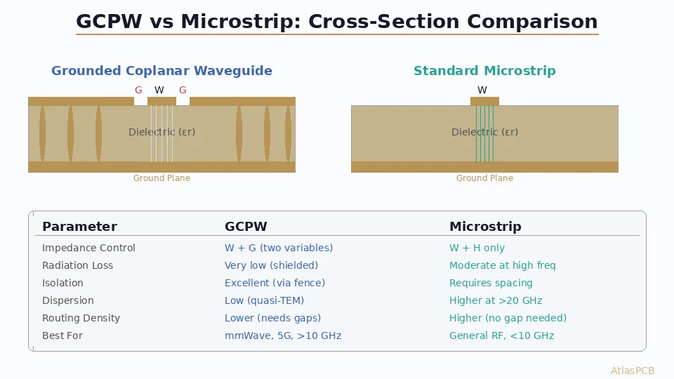
Microstrip
- Trace on outer layer, ground plane below
- Most common RF structure
- Easy to probe and tune
- Higher radiation at high frequencies
Grounded Coplanar Waveguide (GCPW)
- Trace with ground copper on both sides (same layer) + ground plane below
- Better ground return path than microstrip
- Less radiation
- Preferred for >10 GHz designs and connectors
Stripline
- Trace between two ground planes
- Best shielding (lowest radiation)
- More difficult to probe
- Used for sensitive RF interconnects between components

RF Layout Best Practices
Grounding
- Continuous ground plane is the single most important rule in RF design
- Via stitching along RF traces (every lambda/20 spacing)
- Ground plane cutouts only where absolutely necessary (filter structures)
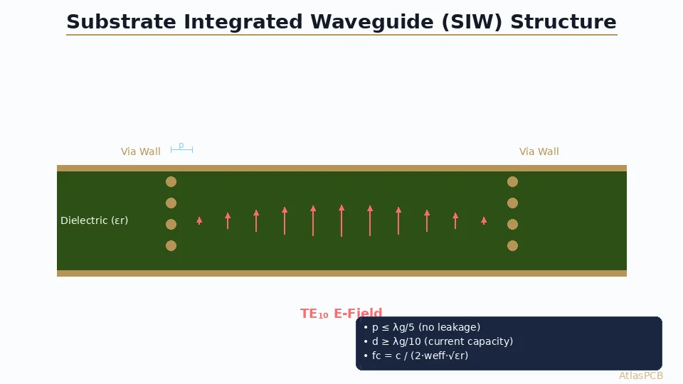
- Via fences around RF sections to isolate from digital
Component Placement
- Keep RF signal path as short as possible
- Place matching components (L, C) directly at the RF trace with minimal stubs
- Orient components for straight-through RF flow (minimize bends)
- Separate RF from digital/power sections with ground fencing
Trace Routing
- No 90-degree bends — use 45-degree mitered bends or curved traces
- Maintain constant trace width through the entire RF path
- Minimize via transitions (each via adds ~0.1-0.3nH inductance)
- Length matching for phased arrays must be within lambda/100
Matching Networks
- Place matching components as close to the IC pin as possible
- Use 0402 or 0201 components for frequencies >5 GHz (smaller parasitics)
- Account for pad parasitic capacitance in matching calculations
- Use EM simulation (HFSS, CST, Sonnet) for >10 GHz designs
RF Connectors and Transitions
| Connector | Max Frequency | Impedance |
|---|---|---|
| SMA | 18 GHz | 50 ohm |
| 2.92mm (K) | 40 GHz | 50 ohm |
| 2.4mm | 50 GHz | 50 ohm |
| 1.85mm (V) | 65 GHz | 50 ohm |
| U.FL/IPEX | 6 GHz | 50 ohm |
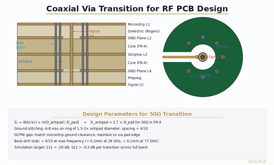
Launch Design
The transition from connector to PCB trace (the “launch”) is critical:
- Match the connector’s field pattern to the PCB transmission line
- Use ground vias near the signal pin to control impedance
- Taper the trace width if needed for impedance matching
- EM simulate the launch for frequencies >10 GHz
Manufacturing Considerations
Copper Surface Roughness
At high frequencies, current flows in a thin skin depth layer on the copper surface. Rough copper increases the effective path length and signal loss.
- Standard ED copper: Rz ~6-8um. Acceptable to ~5 GHz.
- RTF (Reverse Treated Foil): Rz ~3-4um. Good to ~20 GHz.
- VLP (Very Low Profile): Rz ~1-2um. Required for >20 GHz.
Etching Precision
- RF trace width tolerance should be +/-10% or tighter
- Automated process control with AOI verification
- Etch compensation for thick copper
Via Plating
- Via hole diameter and plating uniformity affect via impedance
- Ground via arrays near RF vias are critical
- Back-drilling for through-hole vias if stub resonance is a concern
Conclusion
RF/microwave PCB design combines electromagnetic theory with practical manufacturing knowledge. Material selection sets the performance ceiling, while layout execution determines whether you reach it. For designs above 10 GHz, EM simulation is essential — analytical formulas are insufficient. Work with manufacturers experienced in RF fabrication, as their process capabilities (copper roughness, etching precision, via plating uniformity) directly impact RF performance.
Further Reading
[RF PCB Design Guidelines: Layout, Grounding & Material Selection]/blog/rf-pcb-design-guidelines/)
[RF PCB Materials Comparison: FR4 vs Rogers vs Taconic vs Isola]/blog/rf-pcb-materials-comparison/)
[RF PCB Manufacturer: What to Look For in a High-Frequency Board Supplier]/blog/rf-pcb-manufacturer/)
[PCB Grounding Techniques: Star, Split, and Solid Ground Plane Strategies]/blog/pcb-grounding-techniques/)
[HDI PCB Design Guide: Stackup Rules, Via Structures & DFM Checklist]/blog/hdi-pcb-design-guide/)
[Rogers 4350B vs FR4: When to Upgrade Your PCB Material]/blog/rogers-4350b-vs-fr4/)
About AtlasPCB — We specialize in complex PCB manufacturing for HDI, RF, and high-reliability applications. Explore our RF and high-frequency PCB services, or get an Rogers RO4350B PCB manufacturing . Every order includes free engineering review. Get your quote.
Reviewed by AtlasPCB Engineering Team — IPC-certified manufacturing specialists with 15+ years of production experience in HDI, RF, and high-reliability PCB fabrication. Content based on factory floor data and real customer design reviews.
Frequently Asked Questions
What PCB material should I use for RF design?
How does frequency affect PCB material selection?
What is impedance control in RF PCB design?
- RF design
- microwave PCB
- antenna
- 5G