· David Okafor · Engineering · 4 min read
PCB Via Size Guide
Complete guide to PCB via sizing covering mechanical drilled vias, laser-drilled microvias, and buried vias. Includes IPC aspect ratio rules, drill-to-copper clearances, annular ring requirements, and HDI via specifications.
Quick Answer
PCB via sizes range from 0.1mm laser-drilled microvias for HDI designs to 0.6mm+ mechanical drilled vias for standard multilayer boards. The critical design parameter is aspect ratio—via depth divided by drill diameter—which determines plating reliability. IPC-6012 Class 2 allows 8:1 aspect ratio for mechanical vias, while Class 3 limits it to 8:1 with enhanced plating requirements. Microvias (IPC-2226 Type I) are limited to 1:1 aspect ratio for single-layer laser drilling. Atlas PCB supports mechanical vias down to 0.15mm and laser microvias down to 0.075mm with copper-filled via capability.
PCB Via Size Guide: Mechanical, Laser & Microvia Dimensions
Via selection is one of the earliest design decisions that constrains your entire PCB layout. Choose vias that are too large and you waste precious routing space—especially critical under fine-pitch BGAs. Choose vias that are too small and you push into HDI territory with associated cost premiums. Get the aspect ratio wrong and your board fails reliability testing.
This guide provides the complete specification framework for PCB via sizing—from standard 0.3mm mechanical vias through 0.075mm laser microvias—covering dimensional requirements, IPC standards, plating considerations, and the manufacturing capabilities that determine what’s actually producible.
Via Size Categories
Standard Mechanical Vias
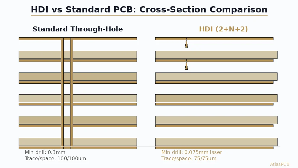
Mechanical drilling uses carbide drill bits to create through-holes and is the most cost-effective via formation method.
| Parameter | Economy | Standard | Advanced |
|---|---|---|---|
| Minimum drill diameter | 0.3mm (12 mil) | 0.2mm (8 mil) | 0.15mm (6 mil) |
| Drill tolerance | ±0.05mm | ±0.05mm | ±0.025mm |
| Minimum annular ring | 0.15mm | 0.125mm | 0.1mm |
| Minimum pad diameter | 0.6mm | 0.45mm | 0.35mm |
| Maximum aspect ratio | 8:1 | 10:1 | 12:1 |
| Typical application | Consumer, IoT | Industrial, telecom | Server, networking |
Standard recommendation: 0.25–0.3mm drill diameter with 0.5–0.55mm pad for general-purpose designs. This provides reliable manufacturing with nearly all PCB fabricators worldwide.
Laser-Drilled Microvias
Laser drilling (UV or CO2) creates vias spanning 1–2 layers, enabling HDI construction:
| Parameter | Standard Microvia | Advanced Microvia |
|---|---|---|
| Drill diameter | 0.1mm (4 mil) | 0.075mm (3 mil) |
| Capture pad | 0.25mm | 0.2mm |
| Target pad | 0.2mm | 0.15mm |
| Maximum depth | 1 layer (typ. 0.06–0.08mm) | 1 layer |
| Aspect ratio | 0.8:1 | 0.75:1 |
| Fill requirement | Copper or conductive epoxy | Copper fill mandatory |
Microvias are the foundation of [HDI PCB design]/blog/hdi-pcb-design-guide/). They enable BGA breakout at 0.5mm pitch and below, where mechanical vias cannot physically fit between pads.
Buried Vias
Buried vias connect inner layers without extending to the outer surfaces:
| Parameter | Specification |
|---|---|
| Minimum drill | 0.15mm (mechanical) |
| Aspect ratio limit | 8:1 (Class 2), 6:1 recommended (Class 3) |
| Registration | ±2 mil to inner layer pads |
| Sequential lamination | Required |
Buried vias add manufacturing complexity and cost but enable higher routing density in thick multilayer boards. See our [blind via vs buried via comparison]/blog/blind-via-vs-buried-via/) for detailed tradeoff analysis.
Aspect Ratio: The Critical Design Constraint
Understanding Aspect Ratio Limits
The aspect ratio (board thickness ÷ drill diameter) determines how effectively the via barrel can be electroplated:
| Aspect Ratio | Plating Challenge | Typical Minimum Thickness at Barrel Center |
|---|---|---|
| 4:1 | Easy | 30+ μm |
| 6:1 | Moderate | 25–28 μm |
| 8:1 | Challenging | 20–25 μm |
| 10:1 | Difficult | 18–22 μm |
| 12:1 | Very difficult | 15–20 μm |
IPC-6012 Class 3 requires minimum 25 μm copper plating at the barrel center. For a 2.4mm thick 16-layer board, the minimum via drill to maintain 8:1 aspect ratio is:
Minimum drill = 2.4mm / 8 = 0.3mm
Aspect Ratio by Board Thickness
| Board Thickness | Min Via (8:1) | Min Via (10:1) | Min Via (12:1) |
|---|---|---|---|
| 1.0mm | 0.125mm | 0.1mm | 0.083mm |
| 1.6mm | 0.2mm | 0.16mm | 0.133mm |
| 2.0mm | 0.25mm | 0.2mm | 0.167mm |
| 2.4mm | 0.3mm | 0.24mm | 0.2mm |
| 3.0mm | 0.375mm | 0.3mm | 0.25mm |
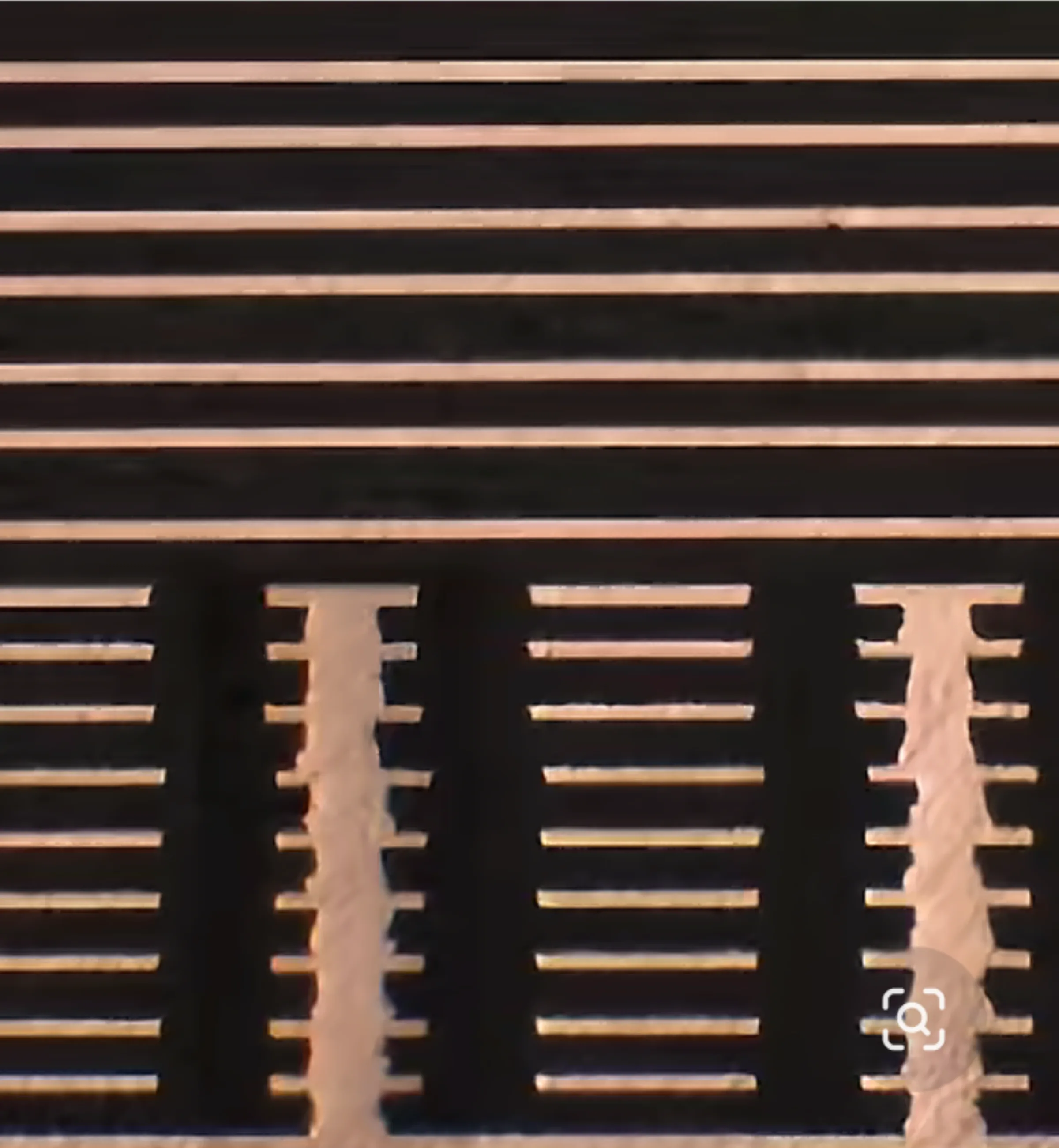
For thick boards requiring small vias, [HDI stackup construction]/blog/hdi-pcb-stackup-design-advanced/) with blind/buried vias is the solution—breaking the via into shorter segments that each meet aspect ratio limits.
Annular Ring Requirements
The annular ring is the copper ring surrounding the drilled hole on each layer. IPC standards define minimum widths:
| Standard | External Layers | Internal Layers |
|---|---|---|
| IPC-6012 Class 1 | 0.05mm (2 mil) | 0.0mm (breakout OK) |
| IPC-6012 Class 2 | 0.05mm (2 mil) | 0.025mm (1 mil) |
| IPC-6012 Class 3 | 0.05mm (2 mil) | 0.05mm (2 mil) |
Practical minimum: Design with 0.1mm (4 mil) annular ring on inner layers and 0.125mm (5 mil) on outer layers to account for drilling registration tolerance. For a 0.3mm drill:
- Minimum pad diameter (Class 2): 0.3 + 2×0.05 + drill tolerance = 0.45mm
- Recommended pad diameter: 0.3 + 2×0.125 = 0.55mm
Via Fill Options by Size
| Via Diameter | Non-conductive Fill | Conductive Epoxy | Copper Fill |
|---|---|---|---|
| 0.075mm | N/A | Possible | Standard |
| 0.1mm | Possible | Standard | Recommended |
| 0.15mm | Standard | Recommended | Optional |
| 0.2mm | Standard | Standard | Premium |
| 0.3mm | Standard | Standard | Premium |
| 0.4mm+ | Standard | Possible | Difficult |
Copper-filled vias (IPC-4761 Type VII) provide the best thermal and electrical performance but become increasingly expensive above 0.2mm diameter. For [thermal via applications]/blog/pcb-thermal-via-design/), copper fill is strongly recommended regardless of via size.
Design Decision Matrix
| Design Requirement | Recommended Via | Pad Size | Notes |
|---|---|---|---|
| General routing | 0.3mm mech. | 0.55mm | Universal compatibility |
| Dense routing | 0.2mm mech. | 0.45mm | Most fabricators |
| 0.8mm BGA | 0.2mm mech. | 0.4mm | Dog-bone breakout |
| 0.5mm BGA | 0.1mm laser | 0.25mm | Via-in-pad, HDI |
| 0.4mm BGA | 0.075mm laser | 0.2mm | Advanced HDI |
| Thermal pad | 0.3mm mech. | 0.55mm | Filled recommended |
| RF/microwave | 0.2mm mech. | 0.4mm | Minimize parasitics |
Ready to optimize your via design? Upload your Gerbers for a free DFM review including via sizing verification.
Further Reading
- [HDI PCB Design Guide: Stackup Rules, Via Structures & DFM Checklist]/blog/hdi-pcb-design-guide/)
- [Blind Via vs Buried Via: Design Rules, Cost Impact & When to Use Each]/blog/blind-via-vs-buried-via/)
- [PCB Thermal Via Design: Engineering Guide]/blog/pcb-thermal-via-design/)
- [Via-in-Pad Design: Filled, Capped, and Plated Over]/blog/via-in-pad-design/)
About AtlasPCB — We specialize in complex PCB manufacturing for HDI, RF, and high-reliability applications. Explore our HDI PCB manufacturing capabilities . Every order includes free engineering review. Get your quote.
Reviewed by AtlasPCB Engineering Team — IPC-certified manufacturing specialists with 15+ years of production experience in HDI, RF, and high-reliability PCB fabrication. Content based on factory floor data and real customer design reviews.
Frequently Asked Questions
What is the minimum via size for standard PCB manufacturing?
What is via aspect ratio and why does it matter?
When should I use microvias instead of mechanical vias?
- via-design
- hdi-pcb
- drilling
- pcb-design