· Priya Nair · Engineering · 5 min read
PCB Testing Methods
A complete guide to PCB testing methods — Automated Optical Inspection, In-Circuit Test, flying probe, functional testing, X-ray inspection, and when to use each approach.

Quick Answer
PCB testing methods include electrical testing (flying probe, bed of nails), visual inspection (AOI), X-ray inspection (for BGA and hidden joints), impedance testing (TDR), and reliability testing (thermal cycling, vibration). 100% electrical testing is standard for production boards.
Testing is the final quality gate before a PCB reaches the end product. Different testing methods catch different types of defects, and the right combination depends on your production volume, board complexity, and reliability requirements.
Bare Board Testing (Before Assembly)
Continuity and Isolation Testing
Every fabricated PCB should be tested for electrical correctness before component assembly.
Flying Probe Test:
- Two or more motorized probes move across the board surface
- Tests each net for continuity (connections exist) and isolation (no shorts)
- No fixture required — ideal for prototypes and small batches
- Speed: 5-50 test points per second
- Cost: $0.50-5.00 per board (depending on complexity)
Fixture-Based (Bed of Nails) Test:
- Custom fixture with spring-loaded pins contacts all test points simultaneously
- Tests all nets in parallel — extremely fast (seconds per board)
- Fixture cost: $500-3,000 (amortized over production volume)
- Speed: 1-5 seconds per board
- Best for: High-volume production (>500 boards)
Impedance Testing (TDR)
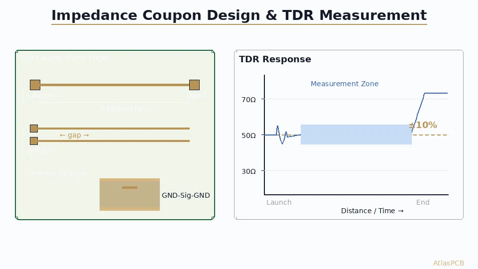
For controlled impedance boards, TDR (Time Domain Reflectometry) verifies that impedance values meet specifications. Test coupons on the panel edge are measured and documented.
Post-Assembly Testing
AOI (Automated Optical Inspection)
How it works: High-resolution cameras capture images of the assembled board from multiple angles. Software compares these images against the expected component placement and solder joint appearance.
What AOI catches:
- Missing components
- Wrong component orientation (polarity)
- Misaligned components
- Solder bridges between pins
- Insufficient solder
- Excess solder
- Tombstoned (lifted) components
- Wrong component values (via marking reading)
What AOI misses:
- Component value errors (a 10K resistor vs 100K looks identical)
- Open solder joints hidden under components (BGA)
- Functional defects (component works but wrong value)
- Internal IC damage
Typical setup: Inline AOI after reflow soldering, before any rework.
Cost: $0.01-0.10 per board (amortized equipment cost)
SPI (Solder Paste Inspection)
Inspects solder paste deposits after stencil printing but before component placement.
Measures: Paste volume, height, area, offset, and bridging. Catching paste defects early prevents downstream assembly failures. ~60% of SMT defects originate from solder paste printing.
X-Ray Inspection
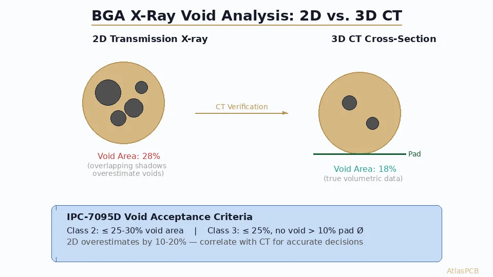
Essential for inspecting solder joints that are hidden from optical inspection.
Primary use: BGA solder ball inspection — verifying ball shape, bridging, voiding, and head-in-pillow defects.
Types:
- 2D X-ray: Quick inspection, shows X-ray shadow image
- 3D CT (Computed Tomography): Slice-by-slice 3D reconstruction — can identify defects at specific BGA ball locations
- Cost: $0.10-1.00 per board (2D), $1-10 per board (3D CT)
ICT (In-Circuit Test)
How it works: A bed-of-nails fixture contacts test points on the assembled board. The ICT system measures:
- Component values (resistance, capacitance, inductance)
- Diode/transistor polarity and forward voltage
- IC pin connectivity
- Short circuits and open circuits
- Voltage at powered test points
Advantages:
- Catches component value errors (10K vs 100K resistor)
- Tests electrical characteristics, not just visual appearance
- High fault coverage (>95% achievable)
- Fast test time (10-30 seconds per board)
Disadvantages:
- Requires custom fixture ($3,000-15,000)
- Requires test point access on the board (DFT — Design for Test)
- Not suitable for prototype or small batch
- Cannot test firmware/software functionality
Best for: Medium to high volume production (>1,000 units)
Flying Probe Test (Post-Assembly)
Similar to bare-board flying probe but performed on assembled boards.
Advantages: No fixture cost, good for prototypes and small batches. Disadvantages: Slow (2-5 minutes per board), limited to DC measurements.
Functional Test (FCT)
How it works: The assembled board is powered up and tested for correct functionality. This may include:
- Power supply voltage verification
- Communication interface testing (UART, SPI, I2C, USB, Ethernet)
- Sensor readings validation
- LED/display verification
- Motor/actuator control testing
- Firmware programming and verification
Advantages:
- Tests actual product functionality
- Catches defects that other tests miss
- Can test firmware and software
Disadvantages:
- Requires custom test software and hardware
- Development time for test programs
- May not pinpoint the root cause of failures
Burn-In Testing
Boards are operated at elevated temperature (typically 85°C) for extended periods (24-168 hours) to screen out infant mortality failures.
Used for: High-reliability applications (medical, aerospace, automotive).
Testing Strategy by Volume
| Volume | Recommended Testing |
|---|---|
| Prototype (1-10) | Visual inspection + flying probe + functional test |
| Small batch (10-100) | AOI + flying probe + functional test |
| Medium (100-1,000) | AOI + ICT or flying probe + functional test |
| High (1,000-10,000) | SPI + AOI + ICT + functional test + sample X-ray |
| Mass (10,000+) | SPI + AOI + ICT + functional test + statistical X-ray + burn-in (if needed) |
Design for Test (DFT) Best Practices
- Add test points: Minimum 40mil (1mm) pads for ICT probing, accessible on one side
- Test point spacing: Minimum 50mil (1.27mm) center-to-center
- Edge clearance: Keep test points 100mil (2.5mm) from board edges
- Access critical nets: Ensure key power rails, data lines, and component pins have test points
- Fiducials: Include at least 3 fiducial marks for fixture and AOI alignment
- BGA considerations: Add test points for BGA signals that are otherwise inaccessible
- Document test requirements: Include test strategy in the design package
Conclusion
No single test method catches all defects. A well-designed test strategy combines multiple methods — visual inspection for obvious defects, AOI for placement accuracy, X-ray for hidden joints, ICT for component values, and functional testing for system behavior. The investment in testing directly correlates with field reliability and customer satisfaction. Design for testability from the start to keep test costs manageable at any volume.
Further Reading
[Controlled Impedance PCB: Design, Stackup & Testing Explained]/blog/controlled-impedance-pcb/)
[BGA Soldering and Rework: Challenges, Inspection, and Best Practices]/blog/bga-soldering-rework/)
[IPC Class 3 Requirements: The Complete Guide for Designers]/blog/ipc-class-3-requirements/)
About AtlasPCB — We specialize in complex PCB manufacturing for HDI, RF, and high-reliability applications. Explore our full PCB manufacturing capabilities . Every order includes free engineering review. Get your quote.
Reviewed by AtlasPCB Engineering Team — IPC-certified manufacturing specialists with 15+ years of production experience in HDI, RF, and high-reliability PCB fabrication. Content based on factory floor data and real customer design reviews.
Frequently Asked Questions
What is flying probe testing for PCBs?
How is PCB impedance tested?
Do all PCBs need electrical testing?
- pcb testing
- AOI
- ICT
- quality control