· Priya Nair · Engineering · 9 min read
PCB Solder Mask
Everything engineers need to know about PCB solder mask — from LPI and dry film types to application methods, dam design rules, thickness specifications, registration tolerances, and DFM optimization. Covers IPC-SM-840 requirements and practical troubleshooting for fine-pitch BGA designs.

Quick Answer
PCB solder mask is a polymer coating (typically epoxy-based LPI applied by screen printing or curtain coating) that protects copper circuits from oxidation, prevents solder bridging during assembly, and provides electrical insulation. Standard LPI solder mask should be 15-35μm thick over traces and 8-15μm on edges, with registration accuracy of ±2-3 mils for conventional PCBs and ±1 mil for fine-pitch BGA designs using Laser Direct Imaging (LDI) exposure.
What Is Solder Mask and Why Is It Critical?
Solder mask (also called solder resist) is the colored polymer layer covering most of a PCB’s surface. While it might seem like a simple protective coating, solder mask serves multiple critical functions:
- Solder bridging prevention — Prevents molten solder from flowing between adjacent pads during reflow assembly
- Copper protection — Shields copper circuits from oxidation, moisture, and environmental contamination
- Electrical insulation — Provides additional dielectric protection between conductors (rated for 500V-2000V depending on thickness)
- Signal integrity — Acts as conformal coating that maintains controlled impedance of surface traces
- Visual inspection — Color contrast makes PCB inspection easier and enables automated optical inspection (AOI)
This guide covers everything from material selection to manufacturing processes to DFM rules that prevent costly yield issues.
Solder Mask Types
Liquid Photoimageable (LPI) — Industry Standard
LPI solder mask dominates modern PCB manufacturing (>90% market share). It’s a two-component epoxy system that’s applied as a liquid, exposed with UV light through a phototool or LDI system, developed to remove unexposed areas, and thermally cured.
Key properties:
- Dielectric strength: 500-1000V/mil
- Operating temperature: -55°C to +150°C (typical)
- CTE: 60-80 ppm/°C (above Tg)
- Tg: 130-150°C
- Adhesion: >1.0 N/mm (peel strength to copper)
- Flammability: UL 94 V-0
Available colors: Green (standard), black, white, blue, red, yellow, matte green, matte black
Application methods:
- Screen printing (most common)
- Curtain coating (better thickness uniformity)
- Spray coating (for 3D surfaces and heavy copper boards)
Dry Film Solder Mask (DFSM)
Dry film is a pre-formed polymer sheet laminated onto the PCB under heat and pressure, then photo-exposed and developed like LPI.
Advantages over LPI:
- Superior thickness uniformity (±2μm vs ±5μm for LPI)
- Better fine-feature resolution (2 mil dams achievable)
- No tenting issues over through-holes
- Consistent dielectric properties
Disadvantages:
- Higher material cost (3-5× LPI)
- Can’t conform to extreme topography (heavy copper, castellated edges)
- Limited color options (primarily green)
- Requires specialized lamination equipment
When to specify dry film:
- Fine-pitch BGA ≤0.5mm pitch
- High-voltage applications requiring guaranteed dielectric thickness
- RF/microwave boards where consistent dielectric affects impedance
- Automotive/Class 3 applications requiring thickness certification
Peelable Solder Mask (Temporary)
A latex or silicone-based temporary mask applied to protect specific areas during selective soldering or conformal coating. Removed after processing — not a permanent protection.
Epoxy-Screen (Legacy)
Older technology using screen-printed non-photoimageable epoxy. Still used for single-sided boards and very low-cost applications. Cannot achieve fine registration or dam widths below 8 mil.
Application Process (LPI)
Understanding the manufacturing process helps engineers design for manufacturing success:
Step 1: Surface Preparation
- Chemical micro-etch to create 2-4 μm surface roughness (Rz)
- Removes oxidation and organic contamination
- Creates mechanical anchor for solder mask adhesion
- Critical: Insufficient roughness causes delamination; excessive roughness creates thin spots
Step 2: Coating Application
Screen printing (two-pass method):
- First pass: Coat one side, dry at 75°C for 30 minutes (tack-free)
- Flip panel: Coat second side, dry at 75°C for 30 minutes
- Result: 25-35 μm wet-film thickness on flat areas
Curtain coating:
- Panel passes through a “curtain” of flowing solder mask liquid
- More uniform thickness than screen printing
- Better coverage over topography
- Requires additional edge-cleaning step
Step 3: Exposure (Photo-Imaging)
The dried (but uncured) solder mask is exposed to UV light (350-420 nm wavelength):
Conventional exposure: Uses film phototool placed in contact with the panel
- Registration: ±2-3 mil (limited by film dimensional stability)
- Resolution: 3-4 mil minimum dam
- Cost: Lower (reusable film)
Laser Direct Imaging (LDI): Digital exposure without phototool
- Registration: ±0.5-1.0 mil
- Resolution: 2-3 mil minimum dam
- Cost: Higher equipment, but no film cost
- Alignment: Automatic fiducial alignment — best for fine-pitch
Step 4: Development
Unexposed solder mask (pad openings) is washed away with 1% sodium carbonate solution:
- Spray development at 30-35°C
- Development time: 60-90 seconds
- Over-development removes too much material (undermining)
- Under-development leaves residue in pad openings
Step 5: Thermal Cure
Final crosslinking at 150°C for 60-90 minutes:
- Develops full mechanical, chemical, and electrical properties
- Under-cure: Soft mask, poor solvent resistance, thermal stress cracking
- Over-cure: Brittle mask, reduced adhesion, darkened color
Thickness Specifications
Solder mask thickness varies significantly across board topography:
Standard Requirements (Per IPC-SM-840)
| Location | Class 2 Minimum | Class 3 Minimum | Typical Target |
|---|---|---|---|
| Over flat areas | 10 μm | 15 μm | 20-30 μm |
| Over trace tops | 8 μm | 10 μm | 15-25 μm |
| Over trace edges | 5 μm | 8 μm | 10-15 μm |
| Between traces | 15 μm | 20 μm | 25-35 μm |
Why Trace Edges Are Critical
Solder mask naturally thins at trace edges due to surface tension during coating. A 1oz (35μm) copper trace creates a 35μm step that the mask must conform to. The resulting thinning at edges is the #1 cause of solder mask failures:
- Edge coverage = typically 30-50% of flat-area thickness
- A 25μm flat-area coating may only be 8-12μm at edges
- Thinner regions are first to crack during thermal cycling
Design mitigation:
- Specify 30μm minimum flat-area thickness (not 20μm) for 1oz copper
- For 2oz copper, increase to 35-40μm or use conformal coat supplement
- Avoid routing traces directly under BGA arrays where edge thinning + mechanical stress combine
Fine-Pitch BGA Design Needs Precision Solder Mask?
AtlasPCB uses LDI exposure for ±1 mil solder mask registration and 2.5 mil minimum dam widths — critical for 0.4-0.5mm pitch BGA reliable assembly.
Request a DFM Review →Solder Mask Dam Design Rules
The solder mask dam — the strip of mask between adjacent pad openings — is often the most challenging feature to manufacture reliably.
Minimum Dam Width by Technology
| Manufacturing Method | Absolute Minimum | Reliable Minimum | Recommended |
|---|---|---|---|
| Screen print (film) | 3 mil (75μm) | 4 mil (100μm) | 5+ mil (125μm) |
| LDI exposure | 2 mil (50μm) | 3 mil (75μm) | 4+ mil (100μm) |
| Dry film | 2 mil (50μm) | 2.5 mil (63μm) | 3+ mil (75μm) |
BGA Pad Pitch vs. Dam Width
For a solder-mask-defined design:
| BGA Pitch | Pad Diameter | Mask Opening | Dam Width Available |
|---|---|---|---|
| 1.27mm | 0.6mm (24 mil) | 0.7mm (28 mil) | 0.57mm (22 mil) ✓ |
| 1.0mm | 0.5mm (20 mil) | 0.6mm (24 mil) | 0.4mm (16 mil) ✓ |
| 0.8mm | 0.4mm (16 mil) | 0.5mm (20 mil) | 0.3mm (12 mil) ✓ |
| 0.65mm | 0.33mm (13 mil) | 0.43mm (17 mil) | 0.22mm (8.6 mil) ✓ |
| 0.5mm | 0.25mm (10 mil) | 0.3mm (12 mil) | 0.2mm (8 mil) ⚠️ |
| 0.4mm | 0.2mm (8 mil) | 0.25mm (10 mil) | 0.15mm (6 mil) ⚠️ |
For pitches ≤0.5mm, consider:
- Eliminating the dam entirely (mask-in-between removed)
- Using NSMD pads with reduced clearance
- Applying solder paste stencil control instead of relying on mask dams
Dam Integrity and Failure Modes
When dams are too narrow, common failures include:
- Dam peeling — Insufficient adhesion area causes delamination during thermal cycling
- Solder wicking — Capillary action draws solder under lifted dam edges
- Bridge defects — Missing dam allows solder paste to spread between pads
- Inspection escapes — Narrow dams are difficult to verify in AOI
Registration and Alignment
Registration Sources of Error
Total registration error is the RSS (root sum of squares) of multiple contributors:
| Error Source | Magnitude (typical) | Notes |
|---|---|---|
| Film dimensional stability | ±1.5 mil | Temperature/humidity dependent |
| Exposure alignment | ±0.5-1.0 mil | LDI vs contact |
| Panel stretch (lamination) | ±1.0 mil | Varies by panel size |
| Development undercut | ±0.5 mil | Process-dependent |
| Total (RSS) | ±2.0-2.5 mil | Film exposure |
| Total (LDI) | ±1.0-1.5 mil | Direct imaging |
Design Rules for Registration
- Standard PCB (film exposure): Design with ±3 mil clearance between pad edge and mask edge
- Fine-pitch (LDI): Design with ±1.5 mil clearance
- Critical applications: Add ±0.5 mil additional margin for safety
Mask Expansion (Solder Mask Clearance)
The mask opening is always larger than the copper pad to prevent mask encroachment:
| Application | Recommended Expansion | Per Side |
|---|---|---|
| Standard SMD pads | 3-5 mil total | 1.5-2.5 mil/side |
| Fine-pitch (≤0.5mm) | 2-3 mil total | 1.0-1.5 mil/side |
| Through-hole pads | 4-6 mil total | 2-3 mil/side |
| Thermal pads | 5-10 mil total | 2.5-5 mil/side |
Solder Mask for Specific Applications
High-Voltage Isolation
For boards with high-voltage requirements (>500V), solder mask provides supplementary insulation but should never be the primary isolation barrier:
- Minimum mask thickness for voltage isolation: 25μm per 500V (conservative)
- Creepage requirements (per IPC-2221): Defined by conductor spacing, not mask
- Conformal coating should supplement solder mask for harsh environments
RF and High-Frequency Boards
Solder mask affects impedance of surface microstrip traces:
- LPI solder mask has εr ≈ 3.5-4.0 and loss tangent (Df) ≈ 0.02-0.03
- At 10+ GHz, solder mask loss becomes significant
- Options: Remove mask over RF traces, use low-loss mask (Df < 0.01), or design impedance with mask included
Impedance impact: A 50Ω microstrip designed without mask consideration will shift to ~47-48Ω when 25μm of mask is applied. Account for this in stackup calculations or remove mask from critical RF traces.
Flex and Rigid-Flex PCBs
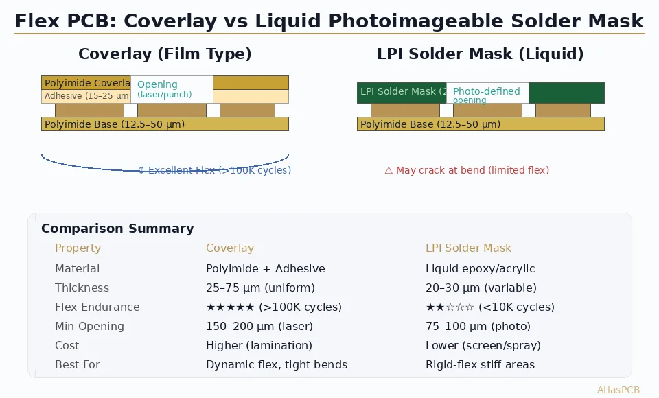
Flexible circuits use coverlay (polyimide film adhesive laminate) instead of LPI solder mask in bend areas:
- Coverlay: Polyimide (25μm) + adhesive (25μm), applied by hot press
- LPI on flex: Acceptable only in non-bend areas
- Bend areas require coverlay for mechanical reliability (LPI would crack)
Heavy Copper (3oz+) Boards
High-copper-weight boards present unique challenges:
- 3oz copper = 105μm step height — mask thinning at edges is severe
- Solution: Apply multiple coats (two-pass screen print) or use spray coating
- Alternative: Specify thicker total mask (40-50μm flat-area minimum)
- Post-processes like edge filling may be needed for reliable coverage
Troubleshooting Common Solder Mask Issues
Issue: Solder mask on pad (SMOD)
Cause: Registration error or under-exposure/over-development Effect: Reduces solderable area, potential tombstoning on small components Fix: Increase mask clearance, switch to LDI, verify development parameters
Issue: Solder bridging during assembly
Cause: Missing or insufficient dam between pads Effect: Short circuits, rework required Fix: Verify dam width in design meets process capability, check for dam peeling
Issue: Mask peeling after reflow
Cause: Insufficient cure, contaminated copper surface, CTE stress Effect: Exposed copper, cosmetic failure, potential long-term reliability issue Fix: Verify cure profile (150°C/60min minimum), check micro-etch process, consider lower-CTE mask material
Issue: Bubbles/fish-eyes in mask
Cause: Trapped air or moisture in coating, surface contamination Effect: Thin spots or voids in mask, potential insulation failure Fix: Improve pre-cleaning, verify coating equipment parameters, degas material before use
Issue: Color variation across board
Cause: Thickness variation from topography, curing temperature gradients Effect: Cosmetic only (usually), but may indicate process control issues Fix: Optimize coating method for uniform deposition, ensure level oven temperature
IPC-SM-840 Compliance
IPC-SM-840 “Qualification and Performance Specification for Permanent Solder Mask” defines the material qualification requirements:
Key Tests
| Test | Requirement | Method |
|---|---|---|
| Adhesion (tape pull) | No removal | IPC-TM-650 2.4.28 |
| Solder resistance (288°C/10s) | No wrinkling, no peeling | IPC-TM-650 2.4.28 |
| Moisture resistance | No blistering after 168h/85°C/85%RH | IPC-TM-650 2.6.3 |
| Chemical resistance (flux, solvents) | No softening or discoloration | IPC-TM-650 2.3.2 |
| Dielectric withstand | >500V/mil | IPC-TM-650 2.5.7 |
| Flammability | UL 94 V-0 | UL 94 |
Classification Groups
IPC-SM-840 classifies solder mask materials into groups:
- Group SM-T: Thermal cure only (screen-printed epoxy)
- Group SM-P: Photoimageable (LPI)
- Group SM-D: Dry film photoimageable
- Group SM-F: Flexible solder mask
Each group has sub-classifications based on halogen content and RoHS compliance.
DFM Optimization Checklist
Before Sending to Fabrication
- Minimum mask dam ≥4 mil (≥3 mil with LDI confirmation)
- Mask clearance matches registration capability (±3 mil standard, ±1.5 mil LDI)
- NSMD vs SMD pad decision documented for all BGAs
- Through-hole via tenting specified (tenting side, open side)
- Mask color specified in fabrication drawing
- Via-in-pad mask strategy defined (plugged, tented, or open)
- Copper pour under BGA has mask removed for thermal pad (if applicable)
- Edge clearance from board outline: minimum 10 mil
- Fiducials have mask clearance ≥40 mil radius
- Solder mask finish specified (gloss or matte) if cosmetically important
Design Rule Recommendations
| Feature | Standard Board | Fine-Pitch Board | HDI Board |
|---|---|---|---|
| Minimum dam | 4 mil | 3 mil | 2.5 mil |
| Mask clearance | 3 mil/side | 1.5 mil/side | 1 mil/side |
| Via tenting | Both sides | Both sides | Top tent, bottom open |
| Registration method | Film phototool | LDI | LDI |
| Mask type | LPI | LPI (LDI) | Dry film or LPI (LDI) |
Conclusion
Solder mask is far more than a protective coating — it’s a precision-engineered functional layer that directly affects assembly yield, electrical reliability, and product lifetime. Key takeaways:
- Specify your requirements clearly — Registration accuracy, dam width, thickness, and class
- Design for process capability — Know whether your fabricator uses film or LDI exposure
- Account for topography — Edge thinning on traces means flat-area specs understate the challenge
- Validate with your assembler — Solder mask issues become assembly defects — coordinate requirements
At AtlasPCB, our LDI-equipped manufacturing line delivers ±1 mil solder mask registration with verified 2.5 mil minimum dams for fine-pitch BGA designs. Our DFM team reviews every order for solder mask producibility before manufacturing begins. Get your DFM review and quote →
Further reading: [PCB Solder Mask Dam Design Rules (detailed)]/blog/pcb-solder-mask-dam-design-rules-dfm/) | [BGA Pad Design and Via-in-Pad]/blog/bga-pad-design-via-in-pad-solder-voiding-prevention/) | [PCB Surface Finish Comparison]/blog/pcb-surface-finish-enig-hasl-osp-hard-gold-enepig/) | [DFM for Fine-Pitch BGA]/blog/dfm-fine-pitch-bga-pcb-design-rules/)
About AtlasPCB — We specialize in complex PCB manufacturing for HDI, RF, and high-reliability applications. Explore our HDI PCB manufacturing capabilities, free engineering DFM review, or get an full PCB manufacturing capabilities . Every order includes free engineering review. Get your quote.
Reviewed by AtlasPCB Engineering Team — IPC-certified manufacturing specialists with 15+ years of production experience in HDI, RF, and high-reliability PCB fabrication. Content based on factory floor data and real customer design reviews.
Frequently Asked Questions
What is the minimum solder mask dam width between pads?
Should I use solder mask defined (SMD) or non-solder-mask defined (NSMD) pads for BGA?
Why does solder mask crack or delaminate during thermal cycling?
- solder mask
- PCB manufacturing
- LPI
- dry film
- DFM
- fine-pitch BGA
- IPC-SM-840
- solder mask dam
- registration
- PCB fabrication