· Priya Nair · Technical Guide · 17 min read
Solder Mask Dam Design
A comprehensive DFM guide to solder mask dam design covering minimum dam widths by technology, registration tolerances, SMD vs NSMD pad definitions, LPI vs dry film processes, BGA dam design for fine-pitch, via tenting, and IPC-SM-840 compliance.
Quick Answer
Solder mask dam width must equal the fabricator minimum (typically 3-4 mil) plus 2× registration tolerance. Standard LPI with film imaging requires 10 mil Gerber dams; advanced LPI with direct imaging allows 5 mil. For 0.5 mm pitch BGAs, NSMD dams become marginal; switch to SMD pad definition to preserve adequate dam width.
Solder mask is one of the most critical yet frequently misunderstood layers in PCB design. It protects copper from oxidation, prevents solder bridges during assembly, provides electrical insulation between adjacent conductors, and shields the board from environmental contamination. At the heart of solder mask design is the solder mask dam — the strip of mask material between adjacent pad openings — and getting the dam design right is essential for manufacturing yield, especially as component pitches shrink below 0.5 mm.
This guide covers everything PCB designers need to know about solder mask dam design: minimum dam widths across different manufacturing technologies, registration tolerances and their interaction with dam widths, the SMD vs NSMD pad definition choice for BGAs, LPI vs dry film solder mask processes, via tenting and plugging considerations, the impact of mask color on resolution, IPC-SM-840 requirements, and the most common DFM violations we see in production — along with how to fix them.
For a broader overview of solder mask materials and processes, see our [PCB solder mask guide]/blog/pcb-solder-mask-guide/). For comprehensive DFM review practices, refer to our [PCB DFM checklist]/blog/pcb-dfm-checklist/).
Solder Mask Dam Fundamentals
A solder mask dam is the web of cured solder mask material remaining between two adjacent solder mask openings (pad exposures). The dam prevents solder from flowing between pads during reflow, which would create short circuits. The minimum achievable dam width depends on the solder mask material, application method, imaging resolution, and registration accuracy of the fabrication process.
Why Dam Width Matters
If the dam is too narrow, several failure modes can occur:
- Dam collapse during development: The uncured mask in thin dams may not fully polymerize through its thickness, causing the dam to wash away during the alkaline development step.
- Dam lifting during soldering: Thin dams have poor adhesion to the copper/laminate substrate and may delaminate under thermal stress during reflow (260+ °C for lead-free processes).
- Insufficient insulation: Even if the dam survives fabrication and assembly, a very thin dam may not provide adequate electrical insulation, especially in high-humidity environments.
- Solder bridging: If the dam is absent or compromised, molten solder wicks between adjacent pads, creating short circuits that require costly rework or board scrapping.
Conversely, if the designer specifies dams that are wider than necessary, the pad openings must shrink, which can reduce the soldering area, complicate paste printing, and affect solder joint reliability. The goal is to specify the minimum dam width that your fabricator can reliably produce.
Minimum Dam Widths by Technology
Solder mask dam capability varies significantly across fabrication technologies. The following table summarizes industry-standard minimum dam widths:
| Technology | Minimum Dam Width | Typical Application | Notes |
|---|---|---|---|
| Standard LPI | 4 mil (100 µm) | General PCB production | Most fabricators’ standard capability |
| Advanced LPI | 3 mil (75 µm) | Fine-pitch BGA, HDI boards | Requires direct imaging (DI) equipment |
| Premium LPI | 2 mil (50 µm) | Ultra-fine-pitch (≤0.3 mm) | Limited to top-tier fabricators; higher cost |
| Dry Film Solder Mask | 3 mil (75 µm) | Flex circuits, high-aspect via tenting | Better thickness uniformity than LPI |
| Inkjet Solder Mask | 3 mil (75 µm) | Prototyping, quick-turn | Digital process, no film tooling needed |
Critical note: These are design-side minimums — the dam width as drawn in the Gerber data. Due to registration tolerance (discussed below), the actual dam width on the finished board may be narrower. Designers must account for registration tolerance when specifying dam widths.
The Registration Tolerance Factor
Solder mask registration tolerance is the maximum positional error between the solder mask layer and the copper pattern. This error arises from:
- Film tooling dimensional stability (for conventional photo-imaging)
- Alignment accuracy of the exposure equipment
- Substrate dimensional changes during processing (stretching, shrinkage)
- Scaling errors between inner layers and outer solder mask
Typical registration tolerances:
| Method | Registration Tolerance |
|---|---|
| Film-based (conventional) | ±3 mil (75 µm) |
| Direct Imaging (LDI) | ±1 mil (25 µm) |
| Inkjet | ±1.5 mil (38 µm) |
Design rule: The dam width on the Gerber data should be ≥ minimum dam width + 2 × registration tolerance.
Example: For standard LPI with film-based imaging:
- Minimum dam: 4 mil
- Registration: ±3 mil
- Required Gerber dam width: 4 + 2 × 3 = 10 mil
Example: For advanced LPI with direct imaging:
- Minimum dam: 3 mil
- Registration: ±1 mil
- Required Gerber dam width: 3 + 2 × 1 = 5 mil
This is why fine-pitch BGA designs almost universally require direct imaging — the registration tolerance of conventional film-based processes consumes too much of the available dam space.
SMD vs NSMD Pad Definitions
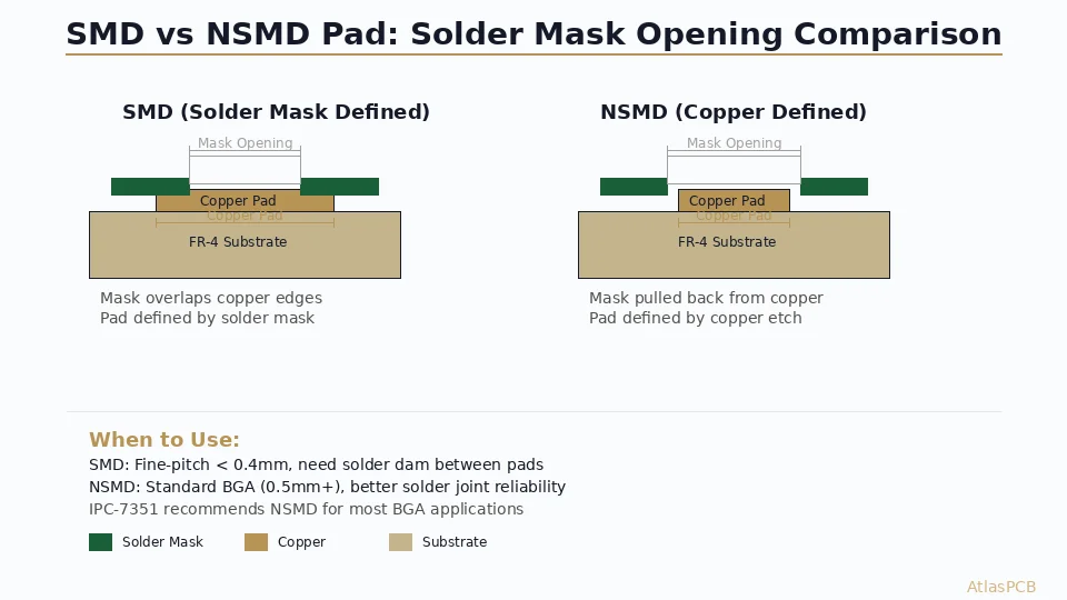
The choice between Solder Mask Defined (SMD) and Non-Solder Mask Defined (NSMD) pads profoundly affects dam design, solder joint reliability, and manufacturing yield for BGA components.
Non-Solder Mask Defined (NSMD) Pads
In NSMD pads (also called copper-defined pads), the solder mask opening is larger than the copper pad. The solder-exposed area is defined by the copper pad geometry, not the mask opening. The mask opening is typically 2–4 mil larger than the pad on each side.
Advantages:
- Larger solder joint area (solder wets the pad edges and sidewalls)
- Stronger solder joints — up to 30% higher shear strength than SMD per industry studies
- Better self-centering during reflow due to full pad wetting
- Industry-preferred for most BGA applications
Disadvantages:
- Requires wider dam widths because the mask opening encroaches into the inter-pad space
- Pad size is limited by the copper etching process, not the more precise mask imaging
- Copper pad edges are exposed and vulnerable to undercutting during etching
Solder Mask Defined (SMD) Pads
In SMD pads, the solder mask opening is smaller than the copper pad. The solder mask overlaps the pad edges, and the solder-exposed area is defined by the mask opening.
Advantages:
- Allows smaller effective pad openings, preserving larger dams between pads
- Essential for ultra-fine-pitch BGA (≤0.4 mm) where NSMD dams would be too narrow
- Tighter pitch capability because the mask (imaged with higher resolution than etched copper) defines the geometry
Disadvantages:
- Smaller solder joint footprint reduces shear strength by 20–30%
- Solder joint forms a “mushroom” shape that concentrates stress at the mask edge
- More susceptible to solder joint cracking under thermal cycling
- May complicate rework due to solder mask overhang on pads
Choosing Between SMD and NSMD for BGA
| BGA Pitch | Recommended Pad Type | Rationale |
|---|---|---|
| ≥0.8 mm | NSMD | Sufficient space for NSMD dams; better reliability |
| 0.65 mm | NSMD (preferred) or SMD | NSMD feasible with DI; SMD if registration is tight |
| 0.5 mm | NSMD (with DI) or SMD | Dam width is the deciding factor — simulate before committing |
| 0.4 mm | SMD (usually required) | NSMD dams too narrow for reliable fabrication |
| 0.3 mm | SMD (mandatory) | No dam possible with NSMD — use SMD or solder mask removal |
For fine-pitch SMT design guidance, see our [PCB SMT pad design for fine-pitch components]/blog/pcb-smt-pad-design-fine-pitch/).
Dam Design for Fine-Pitch BGA
Fine-pitch BGA dam design is one of the most demanding challenges in PCB DFM. Let us walk through the calculations for common pitches.
0.5 mm Pitch BGA — NSMD Approach
Typical 0.5 mm pitch BGA parameters:
- Pad diameter: 0.275 mm (10.8 mil)
- Pad pitch: 0.5 mm (19.7 mil)
- NSMD mask opening: pad + 2 × 2 mil = 0.375 mm (14.8 mil) — 2 mil clearance per side
Available dam space (Gerber): 19.7 mil - 14.8 mil = 4.9 mil
With direct imaging (±1 mil registration): Worst-case dam: 4.9 - 2 × 1 = 2.9 mil
This is below the 3 mil minimum for most processes. Options:
- Switch to SMD pad definition
- Reduce mask clearance to 1.5 mil per side → dam becomes 6.1 mil → worst-case 4.1 mil ✓
- Use a fabricator with 2 mil dam capability (premium process)
0.4 mm Pitch BGA — SMD Approach
Typical 0.4 mm pitch BGA parameters:
- Pad diameter: 0.25 mm (9.8 mil)
- Pad pitch: 0.4 mm (15.7 mil)
- SMD mask opening: pad - 2 × 1.5 mil = 0.175 mm (6.8 mil) — 1.5 mil overlap per side
Available dam space (Gerber): 15.7 mil - 6.8 mil = 8.9 mil
With direct imaging (±1 mil registration): Worst-case dam: 8.9 - 2 × 1 = 6.9 mil ✓
SMD approach works well at 0.4 mm pitch, providing comfortable dam margins even with standard advanced LPI.
Complete Removal — The “No Dam” Option
For the tightest pitches (0.3 mm and below), or when dam widths fall below manufacturable limits, some designers specify complete solder mask removal across the entire BGA field — a single large mask opening exposing all pads. While this eliminates the dam problem, it creates new challenges:
- No solder bridge protection between pads — relies entirely on paste printing accuracy and solder volume control
- Increased risk of pad-to-pad shorts, especially on inner rows where inspection is difficult
- Loss of the insulation benefit of solder mask
- Flux residue cleanup is more difficult in the open field
This approach should only be used when no other option is viable, and assembly processes must be exceptionally well-controlled.
LPI vs Dry Film Solder Mask
The two dominant solder mask technologies — Liquid Photo-Imageable (LPI) and Dry Film — have different characteristics that affect dam design.
LPI (Liquid Photo-Imageable) Solder Mask
LPI is the industry standard for rigid PCBs. It is applied as a liquid (by curtain coating, screen printing, or spray coating), dried to a tack-free state, then exposed to UV light through a phototool (or by direct imaging) to selectively cure the mask. Uncured areas are dissolved in an alkaline developer.
Characteristics relevant to dam design:
- Thickness control: LPI thickness varies with application method and board topography. Typical thickness is 15–30 µm over bare laminate, but can thin down to 5–10 µm over copper features and near pad edges. This thinning reduces dam strength for narrow dams.
- Resolution: Standard LPI with film phototools achieves ~4 mil minimum feature. LPI with LDI achieves 2–3 mil.
- Conformality: LPI conforms to board topography, thinning over raised copper features. This can leave inadequate dam thickness over traces running between pads.
Dry Film Solder Mask
Dry film solder mask is a pre-formed sheet of photosensitive material laminated onto the PCB surface under heat and pressure. It is primarily used for flex circuits and applications requiring uniform thickness.
Characteristics relevant to dam design:
- Thickness uniformity: Dry film maintains consistent thickness regardless of underlying topography. This provides more reliable dam formation at minimum widths.
- Resolution: Comparable to advanced LPI (3 mil minimum dam with direct imaging).
- Adhesion: Dry film adhesion can be problematic on irregular surfaces, especially near via holes and pad edges. Proper surface preparation is critical.
- Cost: Dry film is generally more expensive than LPI for rigid boards.
Recommendation: For most rigid PCB applications, LPI with direct imaging provides the best combination of resolution, cost, and process maturity. Dry film is preferred for flex and rigid-flex circuits, and for applications where mask thickness uniformity is critical.
Via Tenting and Plugging — Interaction with Dam Design
Vias in or near pad fields create solder mask challenges that interact with dam design.
Via Tenting
Tented vias are covered by solder mask without any additional filling. The mask bridges across the via hole, creating a “tent.” Tenting is the default treatment for vias not in pads.
Dam design interaction:
- Vias adjacent to pads consume dam space — the mask must bridge the via AND maintain a dam to the nearest pad opening.
- If a via is too close to a pad, the tent may merge with the pad opening, eliminating the dam.
- Design rule: Maintain minimum 6 mil edge-to-edge clearance between via tent edge and nearest pad opening for reliable dam formation.
Tenting reliability:
- Vias ≤12 mil (0.3 mm) diameter: tent reliably with standard LPI
- Vias 12–16 mil: tent possible but may have pinholes or thin spots
- Vias >16 mil: tenting unreliable — use via plugging
Via Plugging
Plugged vias are filled with epoxy or other fill material and then capped with solder mask or copper. Via plugging is required for:
- Via-in-pad designs (vias within BGA pads)
- Boards requiring hermeticity
- High-reliability applications requiring zero risk of solder wicking through vias
Dam design interaction:
- Plugged vias create a flat surface that supports solder mask. Dam formation over plugged vias is more reliable than over open vias.
- Via-in-pad with cap plating provides the most reliable surface for BGA pad dam design.
For [HDI PCB]/blog/hdi-pcb-manufacturer/) designs with microvias in BGA fields, via plugging is typically mandatory and should be specified from the start of the design.
Solder Mask Color Impact on Resolution
Solder mask color affects imaging resolution and therefore minimum achievable dam width. This is often overlooked in design but matters for fine-pitch applications.
| Color | Relative Resolution | Notes |
|---|---|---|
| Green | Best (baseline) | Most developed chemistry; highest contrast for imaging |
| Dark Green | Very Good | Slight reduction in contrast vs standard green |
| Blue | Good | Comparable to green for most processes |
| Red | Good | Slightly lower contrast than green |
| Black | Fair | Significant contrast reduction; tighter process window |
| White | Fair | Opacity challenges; thicker application needed |
| Matte Black | Poor | Worst resolution; avoid for fine-pitch designs |
| Clear/Transparent | Good resolution but inspection challenges | Used for aesthetic purposes |
Recommendation: For any design with BGA pitches ≤0.5 mm or dam widths ≤4 mil, use green solder mask to maximize manufacturing yield. If an alternative color is required for product branding, verify the fabricator’s minimum dam width capability in that specific color — it may be 1–2 mil wider than their green capability.
IPC-SM-840 Requirements
IPC-SM-840, “Qualification and Performance Specification for Permanent Solder Mask,” is the governing standard for solder mask materials and their performance. Key requirements relevant to dam design:
Class T (Telecommunication) and Class H (High Reliability)
IPC-SM-840 defines two performance classes:
- Class T: Standard industrial and telecommunication applications
- Class H: High-reliability applications (military, aerospace, medical)
Class H imposes stricter requirements on:
- Adhesion (after thermal stress and humidity exposure)
- Insulation resistance (≥10⁸ Ω after 96 hours at 85°C/85% RH at 100 VDC)
- Electro-chemical migration resistance
- Flame resistance (UL 94 V-0)
Minimum Conductor Spacing Under Solder Mask
IPC-SM-840 requires that the solder mask maintain insulation integrity over conductors spaced at the minimum distances specified in IPC-2221/IPC-2222. The solder mask dam width must be sufficient to ensure this insulation even under worst-case registration error.
For standard designs, IPC-2221 specifies minimum conductor spacing based on voltage:
- 0–15 VDC: 5 mil (0.13 mm) minimum spacing
- 16–30 VDC: 5 mil
- 31–50 VDC: 10 mil (0.25 mm)
- 51–100 VDC: 10 mil
- 101–170 VDC: 15 mil (0.38 mm)
The solder mask dam must cover this minimum spacing even at worst-case registration. For most digital designs operating at 3.3 V or below, this is easily met.
Cure Requirements
The solder mask must be fully cured per the manufacturer’s specification. Under-cured mask — which can occur in narrow dams where UV penetration is compromised by adjacent tall features — may fail adhesion, insulation, or chemical resistance tests per IPC-SM-840.
Common DFM Violations and Fixes
Based on production data from thousands of PCB designs, these are the most frequent solder mask dam DFM violations:
Violation 1: Dam Width Below Fabricator Minimum
Problem: Designer specifies 2 mil dams for a fabricator whose capability is 4 mil.
Symptoms: Dams wash out during development, leading to solder bridges. Or fabricator modifies the design without designer approval (increasing mask openings to merge adjacent pads).
Fix: Always confirm the fabricator’s minimum dam width capability before finalizing the design. Build this specification into your design rules from day one, not as a post-layout check.
Violation 2: No Registration Tolerance Allowance
Problem: Designer draws exactly the minimum dam width without accounting for registration error.
Symptoms: Some boards pass, others fail depending on registration variation — intermittent solder bridging in production.
Fix: Add 2× the registration tolerance to the minimum dam width. If unsure of the fabricator’s registration, use ±3 mil as a conservative default (film-based) or ±1 mil (direct imaging).
Violation 3: NSMD Pads on Ultra-Fine-Pitch BGA
Problem: Designer uses NSMD pad definition on a 0.4 mm pitch BGA, resulting in dam widths of 1–2 mil.
Symptoms: Complete dam loss between all pads in the BGA field. Massive solder bridging during assembly.
Fix: Switch to SMD pad definition for BGA pitches ≤0.4 mm. Recalculate the mask opening to achieve at least 4 mil dam width (3 mil with DI and premium process).
Violation 4: Vias Too Close to Pad Openings
Problem: Untented or partially tented vias within 3 mil of pad openings, consuming all dam space.
Symptoms: Solder wicks into via during reflow, creating insufficient solder joints and potential barrel fill. Dam between via and pad is absent.
Fix: Move vias at least 6 mil (edge-to-edge) from pad openings, or specify via plugging for vias that must be closer. For via-in-pad, always specify plug and cap plate.
Violation 5: Solder Mask Slivers
Problem: Narrow solder mask slivers (1–2 mil wide) between non-pad copper features (traces, thermal reliefs) and pad openings.
Symptoms: Slivers delaminate and become debris, contaminating solder joints. Or they curl during soldering and create cosmetic defects.
Fix: Apply a minimum 3 mil mask web rule between any two mask openings, not just between pads. Where slivers are unavoidable, expand the mask opening to eliminate the sliver entirely — it is better to have no dam than a failed dam.
Violation 6: Inconsistent Mask Clearance
Problem: Different mask clearances used for different pad types on the same board, making dam widths unpredictable.
Symptoms: Some areas of the board have comfortable dams while others are at or below the limit.
Fix: Standardize mask clearance across the design: typically 2 mil per side for standard pads, 1.5 mil for fine-pitch. Use a design rule check (DRC) to flag any dam width below the minimum.
Violation 7: Ignoring Copper Features Under Mask Dams
Problem: A trace runs between two pads, directly under the mask dam. The elevated copper makes the mask thinner over the trace, weakening the dam.
Symptoms: Dam appears adequate on Gerber data but fails in production because the mask is thinned to 5 µm over the trace (vs. 20 µm on flat laminate).
Fix: Route traces outside the dam region when possible. If a trace must pass under a dam, increase the dam width by at least 2 mil to compensate for mask thinning. Discuss with your fabricator for specific guidance.
Violation 8: Non-Standard Mask Color for Fine-Pitch Design
Problem: Designer specifies matte black solder mask on a board with 0.5 mm pitch BGAs.
Symptoms: Higher defect rates on fine-pitch dams compared to green mask production. Fabricator struggles to achieve 3 mil dams reliably.
Fix: Use green solder mask for fine-pitch designs. If color is mandatory, increase the minimum dam width by 1–2 mil to account for reduced resolution.
Practical Dam Width Quick-Reference
For rapid design decisions, use this quick-reference chart:
| Component/Feature | Minimum Gerber Dam Width | Assumes |
|---|---|---|
| Standard pitch (≥0.65 mm) pads | 8 mil | Film imaging, ±3 mil registration |
| 0.5 mm pitch BGA (NSMD) | 5 mil | DI, ±1 mil registration |
| 0.5 mm pitch BGA (SMD) | 6 mil | DI, ±1 mil registration |
| 0.4 mm pitch BGA (SMD) | 5 mil | DI, ±1 mil registration |
| Via tent to nearest pad | 6 mil (edge-to-edge) | Via ≤12 mil diameter |
| Trace under dam | 6 mil (add 2 mil to standard) | LPI process |
| Between non-pad features | 4 mil | Standard LPI |
Design Workflow for Solder Mask Dams
Confirm fabricator capabilities early: Before placement and routing, document the fabricator’s minimum dam width, registration tolerance, and imaging method (film vs. DI).
Set design rules accordingly: Configure your EDA tool’s solder mask clearance and minimum dam width rules based on step 1.
Choose SMD vs NSMD per component: For each BGA, calculate the resulting dam width for both NSMD and SMD approaches. Choose the approach that meets dam requirements while maintaining solder joint reliability.
Run DRC focused on mask dams: After routing, run a design rule check specifically targeting solder mask dams. Flag any dam below the minimum.
Review via proximity: Check that all vias near pad fields have adequate clearance or are properly plugged.
Generate optimized Gerber data: Ensure solder mask layers use the correct clearances and that dam widths match the design intent.
Submit for DFM review: Have the fabricator review the design before committing to production. Our DFM review at Atlas PCB catches dam width issues in over 15% of submitted designs.
For a comprehensive fabrication-readiness review, use our [PCB DFM checklist]/blog/pcb-dfm-checklist/). For designs featuring high-density BGA and fine-pitch components, our [HDI PCB manufacturing service]/blog/hdi-pcb-manufacturer/) includes enhanced solder mask dam capability with direct imaging as standard.
Conclusion
Solder mask dam design sits at the intersection of PCB fabrication capability and assembly reliability. As component pitches continue to shrink, the available space for dams decreases, making careful design-for-manufacturing increasingly critical. The key principles are straightforward: understand your fabricator’s capabilities, account for registration tolerance, choose the right pad definition (SMD vs NSMD) based on pitch, and validate dam widths through DRC before releasing to production.
By following the rules, calculations, and best practices in this guide, you can design solder mask dams that are manufacturable, reliable, and cost-effective — avoiding the expensive surprises that dam failures create during assembly. When in doubt, engage your fabricator early: a brief DFM conversation at the design stage prevents costly respins at the production stage.
Further Reading
- [PCB Panelization and Array Design: V-Score vs Tab Routing, DFM Rules, and Cost Optimization]/blog/pcb-panelization-v-score-tab-routing-dfm-cost-optimization/)
- [PCB Manufacturer with Engineering Review: Why Human DFM Audit Matters]/blog/pcb-manufacturer-engineering-review/)
- [阻焊坝设计 — 规则、公差与DFM最佳实践]/blog/pcb-solder-mask-dam-design-rules-dfm/)
- [Aluminum PCB Thermal Design for High-Power LED and Motor Drivers: Material Selection, Stackup, and DFM Guide]/blog/aluminum-pcb-thermal-design-led-motor-driver/)
- [PCB Design for GaN and SiC Power Devices: Thermal Management, Layout Rules, and Material Selection]/blog/pcb-design-gan-sic-power-devices-thermal-layout/)
- Material Options & Capabilities
About AtlasPCB — We specialize in complex PCB manufacturing for HDI, RF, and high-reliability applications. Explore our HDI PCB manufacturing capabilities, free engineering DFM review, or get an full PCB manufacturing capabilities . Every order includes free engineering review. Get your quote.
Reviewed by AtlasPCB Engineering Team — IPC-certified manufacturing specialists with 15+ years of production experience in HDI, RF, and high-reliability PCB fabrication. Content based on factory floor data and real customer design reviews.
Frequently Asked Questions
What is the minimum solder mask dam width for standard LPI processes?
When should I use SMD versus NSMD pad definitions for BGAs?
How does registration tolerance affect solder mask dam design?
Why does solder mask color matter for fine-pitch designs?
- solder mask
- DFM
- PCB design rules
- solder mask dam
- fine-pitch