· David Okafor · Engineering · 4 min read
PCB Panelization: V-Cut vs Tab Routing Guide
Learn PCB panelization methods — V-scoring, tab routing with mouse bites, panel size optimization, fiducials, tooling holes, and depanelization best practices.

Quick Answer
PCB panelization arranges multiple individual boards on a larger panel for efficient manufacturing and assembly. Methods include tab routing (break-away tabs), V-scoring (pre-cut grooves), and mouse bites (perforated breakaway). Panel design affects yield, cost, and depaneling quality.
Panelization combines multiple individual PCBs into a single larger panel for efficient manufacturing and automated assembly. The two main separation methods are V-scoring and tab routing, each with distinct advantages.
Why Panelize?
- Assembly efficiency: Pick-and-place machines handle panels faster than individual boards
- Cost reduction: Fewer handling steps, better material utilization
- Mechanical support: Small or irregularly shaped boards need panel rails for conveyor transport
- Mixed designs: Multiple different boards can share one panel (array panelization)
V-Score (V-Cut)
How It Works
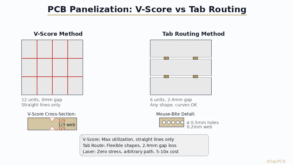
A V-shaped blade scores grooves on the top and bottom of the panel along straight lines. The remaining material (typically 1/3 of board thickness) holds the boards together until snapped apart.
V-Score Specifications
- Groove angle: 30°, 45°, or 60° (30° most common)
- Remaining thickness: 0.3-0.5mm (for 1.6mm board)
- Score line width: ~0.5mm
- Tolerance: +/-0.1mm
Advantages
- Clean, straight edges after separation
- No tab stubs to file or cut
- No stress on components near edges
- Fast depanelization (manual snap or machine)
- Lower cost than tab routing
Limitations
- Straight lines only — cannot accommodate curves or non-rectangular shapes
- Requires 0.3-0.5mm clearance from score line to nearest copper
- Score line must run the full panel length/width (cannot stop mid-panel)
- Slight edge roughness after snapping
Best For
- Rectangular boards
- Boards with no components near edges
- High-volume production where edge quality isn’t critical
Tab Routing (Breakaway Tabs)
How It Works
Individual boards are CNC-routed from the panel, leaving small connecting tabs (bridges) between the boards and the panel frame. Tabs typically include mouse bites (a line of small drilled holes) that create a perforated separation point.
Tab Specifications
- Tab width: 2-5mm (3mm typical)
- Tab count per board: 3-5 minimum for adequate support
- Mouse bite holes: 0.5mm diameter, 0.75mm pitch (typical)
- Hole count per tab: 5-8 holes
Advantages
- Any board shape — handles curves, cutouts, and irregular outlines
- Components can be placed closer to board edges
- More controlled separation with router or laser depanelizer
- Better for boards with edge-mounted components (connectors, switches)
Limitations
- Small tab stubs remain after separation (need filing or routing)
- Mouse bite edges are rougher than V-score
- Slightly higher cost due to CNC routing time
- Tab placement must avoid component footprints
Best For
- Non-rectangular or irregularly shaped boards
- Boards with edge-mounted connectors
- Small boards that need panel support
- Mixed-design panels
Comparison
| Feature | V-Score | Tab Routing |
|---|---|---|
| Board shape | Rectangular only | Any shape |
| Edge quality | Good (clean snap) | Fair (stub residue) |
| Component-to-edge | 0.5mm min | 0.3mm min |
| Depanelization | Manual snap or machine | Router, laser, or manual |
| Cost | Lower | Slightly higher |
| Mechanical stress | Low | Low (with proper tab design) |
| Mixed designs | Limited | Flexible |
Panel Design Best Practices
Panel Frame (Rails)
- Width: 5-8mm on each side (minimum 5mm for assembly conveyor)
- Fiducial marks: 3 minimum — 2 on diagonal corners + 1 on opposite side
- Tooling holes: 2-4 holes (2.0-4.0mm diameter) for fixture alignment
- Bad board marks: X marks for boards that fail testing (assembly machines skip them)
Panel Size Optimization
- Standard panel sizes: 160x100mm, 200x150mm, 250x200mm, 300x250mm
- Maximum assembly panel: Typically 350x250mm (varies by manufacturer)
- Optimal fill ratio: >80% board area to panel area for cost efficiency
- Rotation: Try rotating boards 90° to find the best fit
Component Clearance
- V-score: Keep components >1mm from score line, >0.5mm from copper to score
- Tab routing: Keep components >2mm from tab locations
- No overhanging components into routing paths
Fiducial Marks
- Panel fiducials: 3 minimum, 1mm diameter copper circle with 2mm solder mask opening
- Local fiducials: On each individual board near fine-pitch components (BGA, QFP)
- Placement: Asymmetric to prevent 180° rotation errors
Depanelization Methods
Manual Breaking (V-Score)
- Fastest and cheapest method
- Risk of board flexing — not suitable for ceramic capacitors near edges
- Wear gloves to avoid injury
Automatic V-Score Separator
- Blade runs along the V-score line
- Minimal board stress
- Speed: 100-500mm/s
Router Depanelizer
- CNC router removes tabs with high precision
- No mechanical stress on boards
- Speed: 50-200mm/s
- Best for high-reliability products
Laser Depanelizer
- Non-contact separation — zero mechanical stress
- Best edge quality
- Highest equipment cost
- Used for flex and rigid-flex boards
Conclusion
V-scoring is the default choice for rectangular boards in high-volume production. Tab routing handles everything else — irregular shapes, edge components, and mixed designs. Invest time in panel layout optimization to maximize material utilization and minimize assembly cost. Consult your PCB manufacturer and assembly house early, as their specific panel size preferences and capabilities will influence your panel design.
Further Reading
[PCB Solder Mask: Types, Colors, and Functions Explained]/blog/pcb-solder-mask-guide/)
[Rigid-Flex PCB Design: Stackup, Bend Rules, and Manufacturing Guidelines]/blog/rigid-flex-pcb-design/)
[HDI PCB Design Guide: Stackup Rules, Via Structures & DFM Checklist]/blog/hdi-pcb-design-guide/)
About AtlasPCB — We specialize in complex PCB manufacturing for HDI, RF, and high-reliability applications. Explore our full PCB manufacturing capabilities . Every order includes free engineering review. Get your quote.
Reviewed by AtlasPCB Engineering Team — IPC-certified manufacturing specialists with 15+ years of production experience in HDI, RF, and high-reliability PCB fabrication. Content based on factory floor data and real customer design reviews.
Frequently Asked Questions
What is PCB panelization?
V-score vs tab routing: which is better?
- panelization
- v-cut
- tab routing
- pcb manufacturing