· David Okafor · Engineering · 6 min read
PCB Microsectioning and Cross-Section Analysis
Master PCB microsectioning techniques per IPC-TM-650 2.1.1 — learn sample preparation, polishing procedures, and measurement protocols to verify plating thickness, via quality, and inner-layer registration in production boards.
Quick Answer
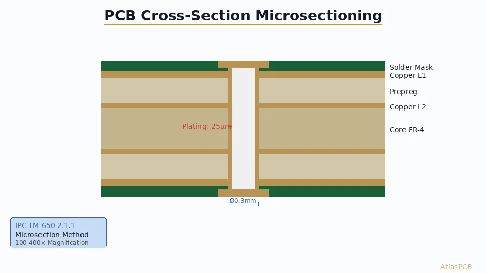
PCB microsectioning is a destructive testing method per IPC-TM-650 2.1.1 that involves encapsulating, grinding, polishing, and examining PCB cross-sections at 100-400× magnification to verify copper plating thickness (typically 20-25μm barrel, ≥5μm knee), inner-layer registration accuracy, and via reliability. It is mandatory for IPC Class 3 qualification and remains the gold standard for validating PCB manufacturing quality.
PCB microsectioning remains the most definitive quality verification method in printed circuit board manufacturing. While automated optical inspection (AOI) and electrical testing catch surface-level defects, only cross-section analysis reveals the true internal construction quality — plating uniformity deep within via barrels, the integrity of copper-to-copper connections at layer transitions, and the precision of inner-layer registration that determines whether your design intent was faithfully reproduced.
For engineers specifying IPC Class 3 reliability requirements — medical devices, aerospace avionics, military electronics — understanding microsectioning is not optional. It’s the evidence that proves your manufacturer meets the tolerances your design demands.
What Is PCB Microsectioning?
Microsectioning (also called metallographic cross-sectioning) is a destructive testing method that involves:
- Cutting a specific area from the PCB panel (usually a dedicated test coupon)
- Encapsulating the sample in epoxy resin
- Grinding and polishing to expose the desired cross-sectional plane
- Examining under optical or electron microscopy at 100-400× magnification
- Measuring critical dimensions against IPC specification limits
The governing standard is IPC-TM-650, Method 2.1.1 — “Microsectioning, Manual Method.” This standard defines the entire workflow from sample preparation through measurement reporting.
Why Destructive Testing Is Still Essential
Despite advances in X-ray CT scanning and non-destructive evaluation, microsectioning provides:
- Direct measurement of plating thickness at barrel, knee, and surface locations
- Visual confirmation of grain structure, voids, and inclusions
- Etch-back and desmear verification impossible to see any other way
- Registration measurement at actual layer interfaces, not extrapolated from external targets
- Court-admissible evidence for failure analysis and warranty disputes
IPC-TM-650 Method 2.1.1: Step-by-Step Process
Sample Selection and Cutting
Test coupons are designed into the PCB panel specifically for microsectioning. They reproduce the same via structures, line widths, and layer stackup as the production boards but are located at panel edges where they can be sacrificed without losing product.
Cutting guidelines:
- Use a precision diamond saw or abrasive cut-off wheel
- Cut at least 5mm away from the target area to avoid mechanical damage
- Avoid generating heat that could delaminate layers (wet cutting preferred)
- Mark the desired polishing plane before encapsulation
Encapsulation
The sample is mounted in clear or colored epoxy resin to:
- Provide rigid support during grinding
- Prevent edge rounding during polishing
- Allow viewing of external layers during progressive grinding
Critical: Use vacuum-assisted encapsulation for through-hole and via samples to prevent air entrapment that can be mistaken for plating voids during inspection.
Grinding and Polishing Sequence
The standard grinding sequence progresses from coarse to fine:
| Step | Abrasive | Purpose |
|---|---|---|
| 1 | 180-240 grit SiC | Approach target plane |
| 2 | 320-400 grit SiC | Remove damage from step 1 |
| 3 | 600 grit SiC | Fine approach |
| 4 | 9μm diamond suspension | Pre-polish |
| 5 | 3μm diamond suspension | Intermediate polish |
| 6 | 1μm diamond or alumina | Final polish |
| 7 | 0.05μm colloidal silica | Mirror finish (optional for SEM) |
Key technique: Rotate the sample 90° between each grit step to confirm that previous grinding marks are completely removed before proceeding.
Etching (Optional)
For copper grain structure analysis:
- Micro-etch: 10% ammonium persulfate solution, 5-10 seconds
- Reveals: Grain boundaries, columnar vs. equiaxed structure, plating interfaces
Critical Measurements in PCB Cross-Sections
Via Barrel Plating Thickness
The most common microsection measurement. IPC-6012 requirements:
| Class | Minimum Barrel Plating | Minimum at Knee |
|---|---|---|
| Class 1 | 20μm (0.8 mil) | No requirement |
| Class 2 | 20μm (0.8 mil) | 5μm (0.2 mil) |
| Class 3 | 25μm (1.0 mil) | 5μm (0.2 mil) |
The “knee” is the critical transition point where the barrel plating meets the inner-layer copper pad. It experiences maximum thermal stress during soldering and is the most common failure point in via reliability.
Inner-Layer Registration
Registration is measured as the offset between the drilled hole center and the target pad center on each inner layer. IPC-6012 Class 3 requires:
- Minimum annular ring remaining: 50μm (2 mil) after drilling
- No drill breakthrough (drill touching inner-layer copper where not intended)
- Maximum offset: defined by pad size minus hole size minus minimum ring × 2
Dielectric Thickness
Prepreg and core thicknesses after lamination must meet design specifications:
- Minimum dielectric spacing between copper layers (typically ≥75μm for standard, ≥50μm for HDI)
- Controlled impedance stackups require ±10% dielectric thickness tolerance
Etch Factor Measurement
The ratio of undercut to etch depth indicates process control:
- Ideal etch factor: 3:1 or better (minimal undercut)
- Measured at trace sidewalls where copper meets dielectric
Microsection Failure Modes: What to Look For
Request a Quote → | View Our Capabilities
Barrel Crack
A circumferential crack in the via barrel plating, typically at the midpoint where thermal expansion stress is maximum. Caused by:
- Insufficient plating thickness
- Excessive Tg differential between resin and copper
- High aspect ratio vias with thin plating at the barrel center
Wedge Void
A triangular void at the via knee where electroless copper failed to uniformly coat the drill smear. Indicates:
- Inadequate desmear processing
- Insufficient catalyst activation
- Drilling heat damage to resin surface
Corner Crack
Stress concentration at inner-layer connections, visible as cracks radiating from the pad corner into the barrel plating. Common in:
- High-reliability applications after thermal cycling
- Lead-free assembly (higher reflow temperatures)
- Small-pad designs with minimal copper reinforcement
Delamination
Separation between copper and dielectric, or between prepreg layers:
- Measles: White spots in the laminate indicating resin fracture
- Pink ring: Oxidized inner-layer copper visible around holes
- Blister: Dome-shaped separation usually moisture-related
Insufficient Wicking (Via Fill)
For via-in-pad designs, the conductive or non-conductive fill must:
- Fill ≥75% of via depth (IPC Class 3)
- Show no center void larger than 25% of via diameter
- Maintain cap plating flatness ≤ 25μm dish or 25μm planar
Equipment and Best Practices
Microscopy Requirements
| Application | Minimum Magnification | Preferred Method |
|---|---|---|
| General plating thickness | 100× | Optical, bright field |
| Knee plating, cracks | 200-400× | Optical with Nomarski DIC |
| Microvia (<100μm) | 500× | Optical or SEM |
| Grain structure | 500-1000× | SEM with EBSD |
| Elemental analysis | 1000× | SEM-EDX |
Measurement Calibration
- Stage micrometer calibration at each magnification
- Minimum 3 measurements per feature, report mean
- Document measurement uncertainty (typically ±1-2μm for optical at 200×)
Digital Documentation
Modern labs use:
- Automated measurement software (image analysis)
- Calibrated digital cameras with scale bars embedded
- Database storage with traceability to panel lot numbers
Microsection Coupon Design Best Practices
Design your test coupons to maximize information:
- Include all via types — through-hole, blind, buried, microvias
- Place coupons at panel corners — worst-case registration locations
- Add daisy-chain test structures — enable electrical correlation
- Design for multiple planes — allow 2-3 successive cross-sections from one coupon
- Include reference dimensions — known features for calibration verification
Coupon Location Strategy
Panel corners experience the greatest registration error due to:
- Material stretching during lamination
- Drill machine positioning accuracy at travel limits
- Inner-layer artwork scaling variation
By placing coupons at corners, your microsection results represent the worst-case condition. If these pass, your production boards will pass.
When to Require Microsectioning
| Scenario | Recommended Samples |
|---|---|
| New design qualification (FAI) | 5-8 coupons across panel |
| IPC Class 3 production | 3 coupons per lot (100% lots) |
| IPC Class 2 production | 1 coupon per lot (sampling plan) |
| Process change validation | 5+ before/after samples |
| Failure analysis | Location-specific from failed unit |
| Customer complaint resolution | Minimum 3 from suspect lot |
Further Reading
- PCB Copper Plating Thickness Uniformity: Electroless vs Electrolytic Processes
- PCB Electrical Testing: Flying Probe vs Fixture Comparison
- Via-in-Pad Plated Over (VIPPO): Design and Manufacturing Guide
Conclusion
PCB microsectioning under IPC-TM-650 remains the irreplaceable quality verification method for confirming internal construction integrity. No amount of electrical testing or X-ray inspection provides the same direct measurement confidence for plating thickness, registration, and structural soundness.
For engineers designing high-reliability products, specify microsection requirements in your procurement documentation. For manufacturers, invest in proper metallographic preparation and calibrated measurement systems. The quality evidence from cross-section analysis is what separates verified reliability from hopeful assumptions.
Need IPC Class 3 PCBs with documented microsection verification? AtlasPCB provides full cross-section reports with every production qualification lot. Get a quote today →
About AtlasPCB — We specialize in complex PCB manufacturing for HDI, RF, and high-reliability applications. Explore our full PCB manufacturing capabilities . Every order includes free engineering review. Get your quote.
Reviewed by AtlasPCB Engineering Team — IPC-certified manufacturing specialists with 15+ years of production experience in HDI, RF, and high-reliability PCB fabrication. Content based on factory floor data and real customer design reviews.
Frequently Asked Questions
What is PCB microsectioning used for?
What magnification is needed for PCB cross-section analysis?
How many microsection samples are needed for IPC Class 3 qualification?
- microsectioning
- cross-section analysis
- IPC-TM-650
- quality control
- via plating
- PCB testing