· Dr. Chen Wei · Engineering · 6 min read
PCB Land Pattern Design
Master IPC-7351B land pattern design for SMD components. Learn density levels, pad dimension calculations, courtyard rules, and thermal relief for optimal PCB assembly yield.
Quick Answer
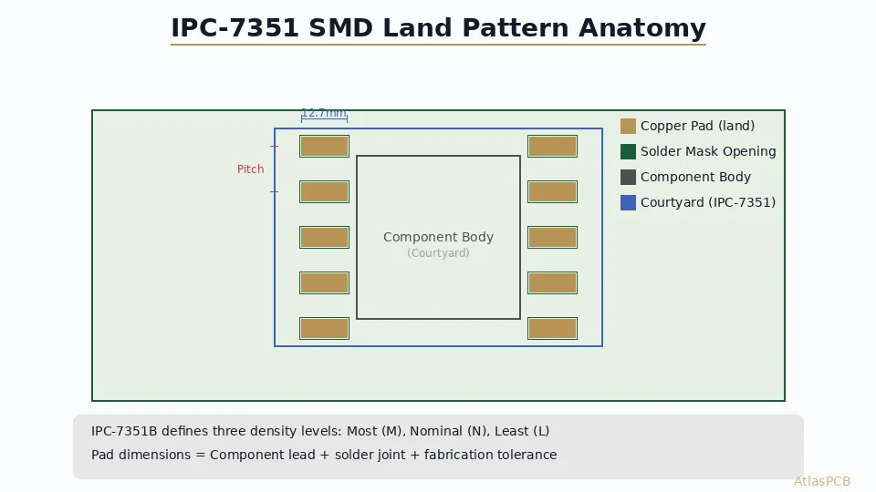
IPC-7351B defines standardized land pattern dimensions for SMD components across three density levels — Most (maximum pads for hand soldering), Nominal (standard production), and Least (minimum for high-density designs) — calculated from component lead geometry plus solder joint requirements plus fabrication tolerances.
Why Land Pattern Design Determines Assembly Yield
The land pattern — also called a footprint or pad pattern — is the copper geometry on a PCB that receives a surface-mount component’s leads or terminations. A correctly designed land pattern ensures:
- Reliable solder joint formation during reflow
- Self-centering of components through surface tension
- Adequate solder fillet size for inspection and reliability
- Sufficient clearance for rework tools
- Compliance with IPC-A-610 workmanship standards
An undersized pad reduces solder joint volume, leading to premature fatigue failures. An oversized pad wastes routing space and can cause bridging on fine-pitch components. IPC-7351B provides the engineering framework to calculate optimal dimensions for any SMD component.
IPC-7351B Fundamentals
Document Scope and History
IPC-7351B (“Generic Requirements for Surface Mount Design and Land Pattern Standard”) is the definitive industry standard for SMD land pattern calculations. It replaced the older IPC-SM-782 standard and provides:
- Mathematical formulas for calculating pad dimensions from component geometry
- Three density-level options for different assembly environments
- Courtyard definitions for component spacing
- Thermal management pad guidelines
- Via-in-pad considerations
The Three Density Levels
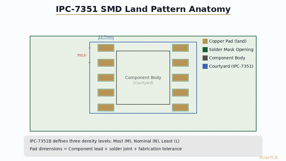
IPC-7351B defines three environment categories that determine pad size extensions:
Level M — Most (Maximum)
- Largest pads, most solder, easiest rework
- Environment: Low-density boards, prototype, hand-assembly
- Courtyard excess: 0.5mm per side
- Toe fillet extension: 0.55mm
Level N — Nominal (Standard)
- Balanced pads for automated production
- Environment: Standard production, reflow soldering
- Courtyard excess: 0.25mm per side
- Toe fillet extension: 0.35mm
Level L — Least (Minimum)
- Smallest pads, maximum routing density
- Environment: High-density, mobile, wearables
- Courtyard excess: 0.1mm per side
- Toe fillet extension: 0.15mm
Pad Dimension Calculation Method
Basic Formula
For a gull-wing lead (QFP, SOP, SSOP):
Pad Length (Z) = Lead Span Max + 2×(Toe Extension) + Tolerance
Pad Width (X) = Lead Width Max + 2×(Side Extension) + Tolerance

Where:
  Toe Extension (Jt) = solder fillet beyond lead toe
  Heel Extension (Jh) = solder fillet at heel
  Side Extension (Js) = solder fillet at sides
  Tolerance = √(component tolerance² + board tolerance² + placement tolerance²)
Extension Values by Component Type
| Component Family | Jt (toe) | Jh (heel) | Js (side) | Notes |
|---|---|---|---|---|
| Gull-wing (QFP) | 0.55/0.35/0.15 | 0.45/0.35/0.25 | 0.05/0.03/0.01 | M/N/L levels |
| J-lead (PLCC) | 0.55/0.35/0.15 | 0.10/0.00/-0.10 | 0.05/0.03/0.01 | Heel under body |
| Chip (0402-2512) | 0.55/0.35/0.15 | 0.00/-0.05/-0.10 | 0.05/0.03/0.01 | Two-terminal |
| BGA | N/A | N/A | N/A | Pad = ball diameter × 0.75-1.0 |
| QFN (exposed pad) | 0.55/0.35/0.15 | 0.00/0.00/0.00 | 0.05/0.03/0.01 | Plus thermal pad |
Worked Example: 0.5mm Pitch QFP-64
Component specifications:
- Lead pitch: 0.5mm
- Lead width: 0.22mm (max 0.27mm)
- Lead length: 0.6mm (max 0.75mm)
- Lead span: 11.75mm - 12.25mm
Nominal (Level N) calculation:
- Pad width = 0.27 + 2×0.03 + 0.05 = 0.38mm → round to 0.35mm
- Pad length = 0.75 + 0.35 + 0.35 + 0.05 = 1.50mm
- Pad center from origin = (12.00/2) + (1.50/2) - 0.75 = 5.25mm
The resulting pad is 0.35mm × 1.50mm centered at 5.25mm from package center.
Courtyard Design Rules
Purpose of the Courtyard
The courtyard defines the minimum area that must remain free around each component. It accounts for:
- Component body overhang
- Lead protrusion beyond body
- Land pattern extent beyond leads
- Assembly tolerance
- Pick-and-place nozzle clearance
- Rework tool access
Courtyard Calculation
Courtyard boundary = Component maximum body dimension
                   + Lead extent beyond body
                   + Courtyard excess (per density level)

Round outward to nearest 0.05mm grid
Let Us Review Your Footprint Library Before Production
AtlasPCB's DFM team validates land patterns against IPC-7351B and our process capabilities. Catch pad errors before they become assembly defects.
Request DFM Review →Courtyard Overlap Rules
When component courtyards overlap:
- Same-side components: Minimum 0.25mm gap between courtyards (Level N)
- Opposing-side components: Courtyards may overlap if thermal profiles are compatible
- Tall components next to short: Consider shadow during wave soldering
Thermal Pad Design for QFN and Exposed-Pad Packages
Ground/Thermal Pad Sizing
QFN and similar packages have a large exposed pad on the bottom for thermal dissipation. IPC-7351B recommends:
- Pad size = 80-100% of exposed pad dimension
- Solder paste coverage: 50-80% of pad area (windowed stencil)
- Via array in thermal pad: minimum 4 vias per 5mm² area
- Via diameter: 0.3mm, plugged with epoxy to prevent solder wicking
Stencil Aperture Design for Thermal Pads
A single large stencil aperture over the thermal pad causes voiding. Best practice:
Aperture design for thermal pad:
- Divide into grid of smaller openings (1.0×1.0mm typical)
- Gap between openings: 0.3-0.5mm
- Total paste area: 50-60% of pad area
- Paste height: 0.125-0.150mm (5-6mil)
This window-pane pattern allows flux gases to escape, reducing void area to < 25% per IPC-7093.
Special Cases and Advanced Topics
0201 and 01005 Components
Ultra-miniature chip components require special attention:
0201 (0.6×0.3mm):
- Pad size: 0.35×0.30mm (Level N)
- Pad gap: 0.20mm
- Solder paste: Type 5 or Type 6
- Stencil thickness: 0.075-0.100mm
01005 (0.4×0.2mm):
- Pad size: 0.25×0.20mm (Level L only)
- Pad gap: 0.15mm
- Solder paste: Type 6 or Type 7
- Requires laser-cut stencil with electroformed apertures
BGA Land Patterns
BGA pad calculation differs from leaded components:
Non-Solder Mask Defined (NSMD):
  Pad diameter = Ball diameter × 0.75 (for 0.5mm pitch)
  Pad diameter = Ball diameter × 0.80 (for 0.8mm+ pitch)
  Solder mask opening = Pad + 0.075mm per side

Solder Mask Defined (SMD):
  Pad diameter = Ball diameter × 1.0
  Solder mask opening = Ball diameter × 0.80
  Used when trace routing between pads is impossible
NSMD pads are preferred because they provide:
- Stronger solder joint (solder wraps around pad edge)
- Better thermal fatigue resistance
- More consistent ball collapse during reflow
Connector and Through-Hole Mixed Technology
For boards with both SMD and through-hole components:
- Through-hole pad annular ring: IPC-6012 minimum per class
- Wave solder side SMD pads: Add 0.1mm to all extensions
- Selective soldering pads: Standard IPC-7351B dimensions apply
- Thermal relief for ground plane connections: 4-spoke, 0.3mm spoke width
Library Naming Convention (IPC-7351B)
IPC-7351B defines a standard naming convention for land patterns:
Format: FAMILY_PINS_BODY-WIDTH_BODY-LENGTH_PITCH_DENSITY

Examples:
  SOIC127P600X175-8N  → SOIC, 1.27mm pitch, 6mm wide, 8 pins, Nominal
  QFP50P1200X1200X160-64N → QFP, 0.5mm pitch, 12×12mm body, 64 pins
  CHIP0805L → 0805 chip component, Least density
  BGA127P13X13_1400X1400X185-169N → BGA, 1.27mm pitch, 13×13 array
This systematic naming enables:
- Unambiguous communication between design and manufacturing
- Automated library management
- DFM rule checking against density level
Common Land Pattern Mistakes
1. Incorrect Component Orientation Mark
The pin-1 indicator must be placed within the courtyard. Ambiguous orientation leads to 180° placement errors — the most common SMT assembly defect.
2. Pad-to-Mask Registration Error
Solder mask registration tolerance is typically ±0.05mm. If pad-to-mask clearance is less than this tolerance, mask may partially cover the pad, causing solder rejection. Minimum solder mask clearance: 0.05mm per side (Level L) to 0.075mm (Level N).
3. Insufficient Pad-to-Pad Gap
Minimum copper-to-copper gap between pads must account for:
- Fabrication etching tolerance (±0.025mm for standard, ±0.015mm for HDI)
- Solder bridging risk (gap < 0.15mm requires solder dam)
- Electrical clearance per IPC-2221 (voltage dependent)
4. Missing Thermal Relief on Power Pads
Large ground/power pads connected to plane layers without thermal relief create a heat sink effect during soldering, causing cold joints. Always specify 4-spoke thermal relief with 0.25-0.30mm spoke width for wave and selective soldering.
Validating Your Land Patterns
Before releasing to fabrication, validate land patterns against:
- Component datasheet — Verify all dimensions match recommended footprint
- IPC-7351B calculator — Check mathematical compliance for chosen density level
- 3D model interference — Confirm component body doesn’t conflict with adjacent parts
- DFM check with fabricator — Verify against actual process capabilities
- Assembly trial — First-article inspection per IPC-A-610
Further Reading
- PCB Solder Paste and Stencil Design Guide
- DFM for Fine-Pitch BGA PCB Design Rules
- AOI and SPI Inspection for PCB Assembly Quality Control
- PCB Design Rules: Trace Width and Spacing
Need land pattern validation for your next production run? AtlasPCB’s DFM engineers review every design against IPC-7351B standards and our manufacturing process windows. Get your free DFM review →
About AtlasPCB — We specialize in complex PCB manufacturing for HDI, RF, and high-reliability applications. Explore our PCB assembly services, free engineering DFM review, or get an full PCB manufacturing capabilities . Every order includes free engineering review. Get your quote.
Reviewed by AtlasPCB Engineering Team — IPC-certified manufacturing specialists with 15+ years of production experience in HDI, RF, and high-reliability PCB fabrication. Content based on factory floor data and real customer design reviews.
Frequently Asked Questions
What are the three density levels in IPC-7351B?
How do I calculate pad dimensions from component specifications?
What is the courtyard in IPC-7351B and why does it matter?
- IPC-7351
- land pattern
- footprint design
- SMD
- PCB assembly
- DFM
- component library