· Sophia Reyes · Engineering · 4 min read
PCB Impedance Control
Understand PCB impedance control — what impedance is, why it needs to be controlled, single-ended vs differential impedance, calculation methods, and testing with TDR.

Quick Answer
PCB impedance control ensures signal traces maintain a specific characteristic impedance (typically 50Ω single-ended or 100Ω differential) to prevent signal reflections and data errors. It is achieved by controlling trace width, dielectric thickness, and copper weight, and verified using TDR (Time Domain Reflectometry) testing.
As signal frequencies increase, controlling the impedance of PCB traces becomes critical. Impedance mismatches cause signal reflections, ringing, and data errors. This guide explains what impedance control is, why it matters, and how to design and verify controlled impedance traces.
What Is Characteristic Impedance?
Characteristic impedance (Z0) is the ratio of voltage to current of an electromagnetic wave traveling along a transmission line. For a PCB trace, it depends on:
- Trace width (W)
- Trace thickness (T) — copper weight
- Dielectric thickness (H) — distance to reference plane
- Dielectric constant (Dk / Er) of the substrate material
- Trace geometry — microstrip (outer layer) vs stripline (inner layer)
Z0 is measured in ohms and is a property of the trace geometry, not the signal itself.
Why Control Impedance?
Signal Reflection
When a signal encounters an impedance discontinuity (change in Z0), part of the signal energy is reflected back toward the source. The reflection coefficient is:
Gamma = (Z_load - Z_source) / (Z_load + Z_source)
A 10% impedance mismatch causes ~5% signal reflection. At high frequencies, these reflections create:
- Ringing: Oscillations on the signal edge that can trigger false logic transitions
- Overshoot/undershoot: Voltage excursions beyond supply rails, potentially damaging ICs
- Data errors: In high-speed serial links, reflections degrade the eye diagram
When Is Impedance Control Needed?
Rule of thumb: Control impedance when the signal rise time is less than twice the propagation delay of the trace.
Practical guideline by interface:
| Interface | Typical Impedance | Control Needed? |
|---|---|---|
| GPIO, I2C (<1 MHz) | N/A | No |
| SPI (<50 MHz) | N/A | Usually no |
| USB 2.0 (480 Mbps) | 90 ohm diff | Yes |
| USB 3.0/3.1 (5-10 Gbps) | 85 ohm diff | Yes (strict) |
| HDMI | 100 ohm diff | Yes |
| Ethernet 100BASE-TX | 100 ohm diff | Yes |
| DDR3/DDR4 | 40-60 ohm SE | Yes |
| PCIe Gen3/4 | 85 ohm diff | Yes (strict) |
| SATA | 100 ohm diff | Yes |
| RF/Microwave | 50 ohm SE | Yes (strict) |
Impedance Types
Single-Ended (SE) Impedance
A single trace referenced to a ground plane. The most common controlled impedance type.
- Standard value: 50 ohm (RF), 60 ohm (general digital)
- Tolerance: +/-10% is standard, +/-5% for high-speed
Differential Impedance
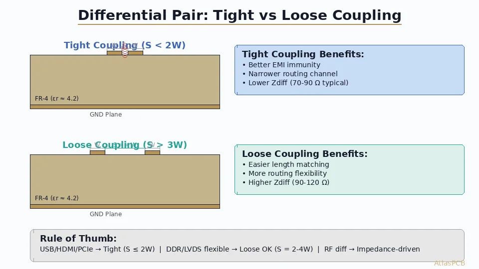
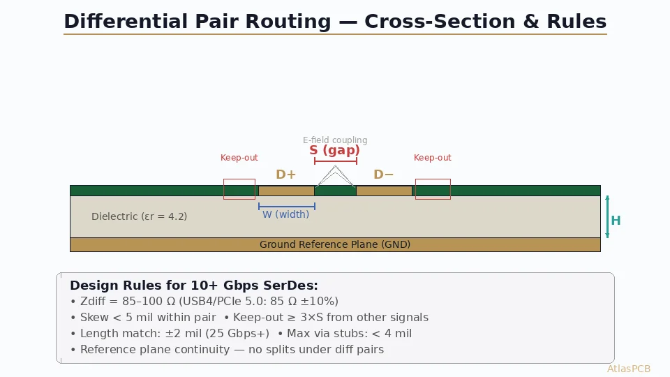
Two traces (a differential pair) carrying complementary signals. The differential impedance is the impedance between the two traces.
- Zdiff ≈ 2 x Z_odd (where Z_odd is the odd-mode impedance of each trace)
- Standard values: 85 ohm (USB3), 90 ohm (USB2), 100 ohm (HDMI, Ethernet, LVDS)
- Coupling matters: Tighter spacing between traces increases coupling and reduces Zdiff
Coplanar Impedance
A trace with ground copper on both sides on the same layer. Used for RF and high-frequency designs where ground return path on the same layer is beneficial.
Trace Geometries
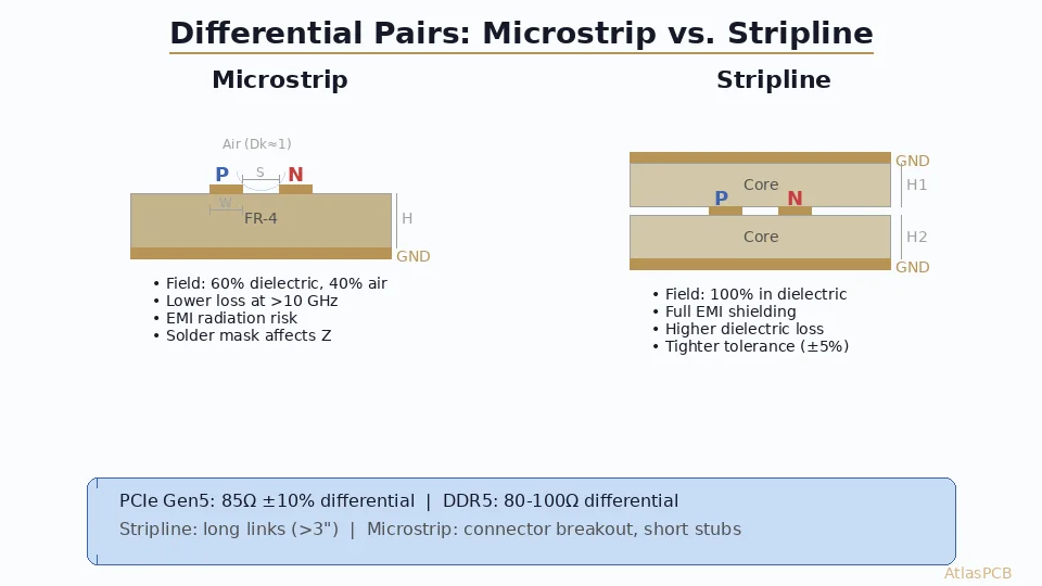
Microstrip
- Trace on an outer layer with a reference ground plane below
- Higher propagation speed (~60% of light speed)
- Slightly higher radiation/EMI
- Easier to probe and debug
Embedded Microstrip
- Outer layer trace covered by solder mask or prepreg
- Dk of solder mask affects impedance (typically Dk~3.5-4.0)
- Most common configuration in real boards
Stripline
- Trace on an inner layer between two ground planes
- Lower propagation speed (~50% of light speed)
- Better shielding — lower EMI
- Used for high-speed inner-layer routing
Impedance Calculation
Key Formula (Microstrip, Approximate)
Z0 ≈ (87 / sqrt(Er + 1.41)) x ln(5.98H / (0.8W + T))
Where:
- Er = dielectric constant
- H = dielectric height (mils)
- W = trace width (mils)
- T = trace thickness (mils)
Practical Examples (FR-4, Dk=4.2, 1oz copper)
50 ohm single-ended microstrip:
| Dielectric Height | Required Trace Width |
|---|---|
| 4 mil (0.1mm) | 7 mil (0.18mm) |
| 5 mil (0.13mm) | 9 mil (0.23mm) |
| 8 mil (0.2mm) | 14 mil (0.36mm) |
| 10 mil (0.25mm) | 18 mil (0.46mm) |
100 ohm differential pair:
| Dielectric Height | Trace Width | Spacing | Pair Gap |
|---|---|---|---|
| 4 mil | 4 mil | 4 mil | 12 mil |
| 8 mil | 7 mil | 6 mil | 20 mil |
| 10 mil | 8 mil | 8 mil | 24 mil |
Use Field Solvers
Approximate formulas are useful for estimation, but production impedance control requires a 2D field solver (e.g., Polar Si9000, Saturn PCB Toolkit, or your EDA tool’s built-in solver) that accounts for:
- Exact trace geometry (trapezoidal cross-section from etching)
- Solder mask effects
- Adjacent trace coupling
- Copper roughness
Impedance Testing with TDR
Time Domain Reflectometry (TDR) is the standard method for verifying controlled impedance:
- A fast-rise-time pulse is sent down the trace
- Reflections from impedance discontinuities are measured
- The impedance profile along the trace length is plotted
- Typical test coupon includes dedicated impedance traces on the panel edge
TDR Test Coupons
- Fabricators include test coupons on each production panel
- Coupons replicate the exact stackup and trace geometries of the production board
- TDR measurement is performed on every panel (or sample-based for high volume)
- Results are documented in an impedance test report
Stackup Impact on Impedance
The PCB stackup directly determines impedance. Key considerations:
- Prepreg/core selection: Different prepreg styles (1080, 2116, 7628) have different thicknesses and Dk values
- Dk tolerance: FR-4 Dk can vary +/-5-10%. Use tighter Dk-tolerance materials for strict impedance control
- Copper roughness: Rougher copper (standard ED) has slightly higher effective Dk than smooth copper (RTF/VLP)
- Symmetric stackup: Always use a symmetric layer arrangement to prevent board warpage and ensure consistent impedance
Conclusion
Impedance control is essential for any design with high-speed digital or RF signals. Work closely with your PCB manufacturer to define the stackup, specify impedance targets and tolerances, and ensure proper test coupons are included. Most manufacturers provide free impedance calculation support — take advantage of this service early in your design process to avoid costly redesigns.
About AtlasPCB — We specialize in complex PCB manufacturing for HDI, RF, and high-reliability applications. Explore our impedance-controlled PCB manufacturing, or get an Megtron 6 & 7 low-loss PCB manufacturing . Every order includes free engineering review. Get your quote.
Reviewed by AtlasPCB Engineering Team — IPC-certified manufacturing specialists with 15+ years of production experience in HDI, RF, and high-reliability PCB fabrication. Content based on factory floor data and real customer design reviews.
Frequently Asked Questions
Why is impedance control important in PCB design?
What is the standard impedance tolerance for PCBs?
How do I calculate PCB trace impedance?
- impedance control
- signal integrity
- differential pair
- high-speed design