· David Okafor · Engineering · 5 min read
PCB Gerber Files
Understand PCB Gerber files — the RS-274X format, ODB++, which layers to include, how to generate them from KiCad, Altium, and Eagle, and common mistakes to avoid.

Quick Answer
Gerber files (RS-274X format) are the industry standard for communicating PCB designs to manufacturers. A complete fabrication package includes copper layers, solder mask, silkscreen, drill files (Excellon), board outline, and a fabrication drawing with stackup and specifications.
Gerber files are the universal language between PCB designers and manufacturers. Getting them right is essential for a smooth fabrication process. This guide explains what Gerber files are, which files you need, and how to generate them correctly.
What Are Gerber Files?
Gerber files are 2D vector image files that describe each layer of a PCB. Each file represents one layer — copper traces, solder mask, silkscreen, paste stencil, etc. The manufacturer’s CAM (Computer-Aided Manufacturing) software reads these files to produce photomasks, drill programs, and other fabrication tools.
Format History
- RS-274D (Standard Gerber): Legacy format with separate aperture files. Mostly obsolete.
- RS-274X (Extended Gerber): Current industry standard. Aperture definitions embedded in the file. Self-contained and unambiguous.
- Gerber X2: Extension of RS-274X with file attributes (layer type, polarity, function). Increasingly adopted.
- Gerber X3: Adds component information. Still emerging.
Always use RS-274X or X2. If your manufacturer requests RS-274D, find a new manufacturer.
Which Files Do You Need?
Standard File Set for a 4-Layer Board
| File | Layer | Extension (typical) |
|---|---|---|
| Top Copper | Front copper traces | .GTL |
| Inner Layer 2 | Ground/power plane | .G2 or .GP1 |
| Inner Layer 3 | Power/signal | .G3 or .GP2 |
| Bottom Copper | Back copper traces | .GBL |
| Top Solder Mask | Front solder mask | .GTS |
| Bottom Solder Mask | Back solder mask | .GBS |
| Top Silkscreen | Front component labels | .GTO |
| Bottom Silkscreen | Back component labels | .GBO |
| Top Paste | Stencil for SMT paste | .GTP |
| Bottom Paste | Stencil for SMT paste | .GBP |
| Board Outline | Board edge definition | .GKO or .GM1 |
| Drill File (PTH) | Plated through-holes | .DRL or .XLN |
| Drill File (NPTH) | Non-plated holes | .DRL or .XLN |
Additional Files
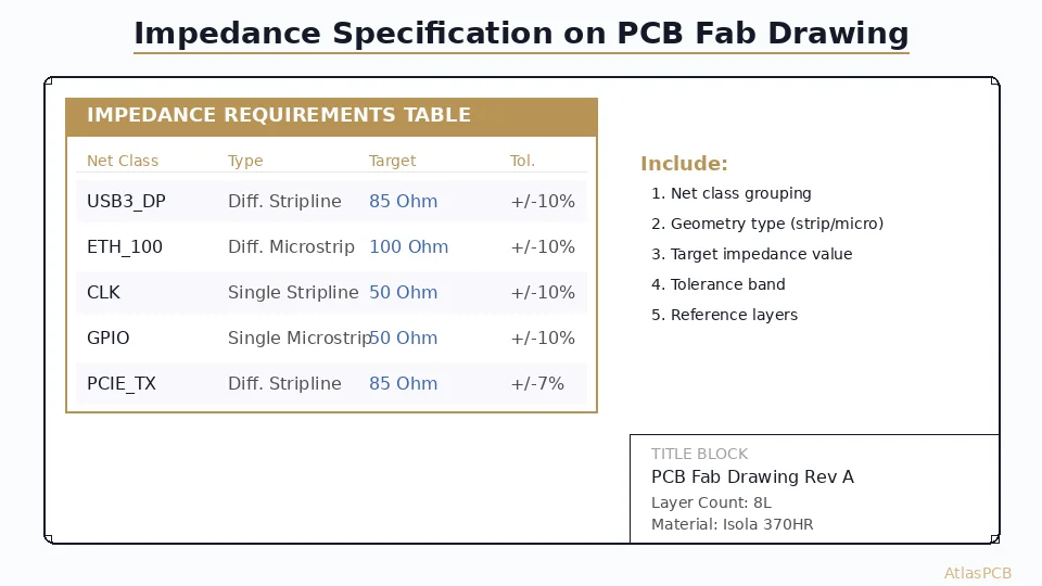
- Fabrication drawing: Dimensions, tolerances, stackup, notes (.GFB or PDF)
- Netlist (IPC-D-356): Electrical netlist for bare board testing
- Pick and place file: Component X/Y coordinates for SMT assembly
- BOM (Bill of Materials): Component list for procurement and assembly
Drill Files
Drill files use the Excellon format (also called NC Drill). They specify:
- Hole locations (X, Y coordinates)
- Hole diameters (tool list)
- Hole types: Plated (PTH) vs Non-Plated (NPTH)
- Drill sequence
Important Settings
- Format: Excellon (2:4 or 2:5 format — 2 integer digits, 4 or 5 decimal digits)
- Units: Metric (mm) preferred; inches also common
- Zero suppression: Leading zero suppression or trailing — must match the file
- Coordinates: Absolute (preferred) or incremental
- Separate files for PTH and NPTH — critical! Non-plated holes must not be copper-plated
Generating Gerbers from Popular EDA Tools
KiCad
- Open PCB Editor → File → Fabrication Outputs → Gerbers
- Select all copper layers + mask + silk + edge cuts + paste
- Format: Gerber X2 (recommended)
- Coordinate format: 4.6 (metric)
- Generate drill files separately: File → Fabrication Outputs → Drill Files
- Format: Excellon, Metric, PTH and NPTH in separate files
Altium Designer
- File → Fabrication Outputs → Gerber Files
- Configure layers in the dialog
- Format: RS-274X
- Units: Metric
- Apertures: Embedded
- File → Fabrication Outputs → NC Drill Files (for drill data)
Eagle
- CAM Processor → Load a Gerber job file (or create new)
- Add all required layers
- Device: GERBER_RS274X
- Generate drill file with EXCELLON device
- Export and verify
ODB++ as an Alternative
ODB++ is a comprehensive single-database format that contains ALL manufacturing data (copper, mask, drill, netlist, stackup, BOM) in one package.
Advantages Over Gerber
- Single file instead of 15-20 separate files
- Includes netlist information (Gerber doesn’t)
- Includes stackup and material specification
- Less room for file mismatch errors
- Increasingly supported by manufacturers
When to Use ODB++
- When your manufacturer supports it (ask first)
- For complex boards with many layers
- When you want to minimize file management errors
Common Gerber Mistakes
1. Missing Board Outline
Without a clear board outline layer, the manufacturer doesn’t know the board shape. Always include a board outline on a dedicated layer (mechanical layer or edge cuts).
2. Wrong Drill File Format
Metric vs imperial mismatch causes holes to be drilled at wrong locations. Always verify units match between Gerber and drill files.
3. Missing Layers
Forgetting to export inner layers, paste layers, or the board outline. Always cross-check your file set against the standard file list.
4. Incorrect Solder Mask Polarity
Solder mask Gerbers can be positive (dark = mask) or negative (dark = opening). Most manufacturers expect positive polarity. Verify by opening in a Gerber viewer.
5. Non-Plated Holes Mixed with Plated
If NPTH and PTH holes are combined in one drill file, the manufacturer may plate holes that should remain unplated (or vice versa). Always generate separate files.
6. Stale/Outdated Files
Re-generate Gerbers every time you make a design change. Don’t send files from an older revision.
Verification Before Sending
Use a Gerber Viewer
Before submitting files, always review them in an independent Gerber viewer:
- Free: KiCad’s GerbView, gerbv, Tracespace.io (online)
- Commercial: CAM350, ViewMate
Verification Checklist
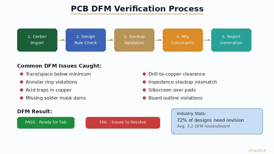
- All copper layers present and correct
- Solder mask openings align with pads
- Silkscreen doesn’t overlap pads
- Board outline is closed and correct dimensions
- Drill holes align with pads
- PTH and NPTH are in separate files
- No stray artifacts or test objects
- Layer count matches your design
Conclusion
Generating correct Gerber files is a critical skill for every PCB designer. Use RS-274X or X2 format, always include complete drill files, verify in an independent viewer, and double-check your file set against the standard list. A few minutes of verification prevents days of delay from manufacturing errors.
Further Reading
[PCB Solder Mask: Types, Colors, and Functions Explained]/blog/pcb-solder-mask-guide/)
[PCB Grounding Techniques: Star, Split, and Solid Ground Plane Strategies]/blog/pcb-grounding-techniques/)
[HDI PCB Design Guide: Stackup Rules, Via Structures & DFM Checklist]/blog/hdi-pcb-design-guide/)
[PCB Manufacturer with Engineering Review: Why Human DFM Audit Matters]/blog/pcb-manufacturer-engineering-review/)
About AtlasPCB — We specialize in complex PCB manufacturing for HDI, RF, and high-reliability applications. Explore our full PCB manufacturing capabilities, or get an instant online quote . Every order includes free engineering review. Get your quote.
Reviewed by AtlasPCB Engineering Team — IPC-certified manufacturing specialists with 15+ years of production experience in HDI, RF, and high-reliability PCB fabrication. Content based on factory floor data and real customer design reviews.
Frequently Asked Questions
What Gerber files do I need for PCB manufacturing?
What is the difference between Gerber and ODB++?
How do I verify my Gerber files before ordering?
- gerber files
- pcb design
- manufacturing data
- CAD