· Thomas Webb · Engineering · 4 min read
PCB Copper Weight and Thickness Explained
Understand PCB copper weight — how oz/ft2 converts to thickness, current carrying capacity for different copper weights, heavy copper PCB applications, and thermal design considerations.

Quick Answer
PCB copper weight is specified in ounces per square foot (oz/ft²), where 1oz equals 35μm (1.4mil) thickness. Standard is 1oz, heavy copper starts at 3oz, and extreme copper exceeds 10oz. Heavier copper carries more current and dissipates more heat but limits trace/space resolution.
Copper weight is a fundamental PCB specification that directly impacts current capacity, heat dissipation, and cost. This guide explains what copper weight means, how it relates to thickness, and when to choose different copper weights.
What Is Copper Weight?
Copper weight refers to the weight of copper per unit area, expressed in ounces per square foot (oz/ft2). This somewhat unusual unit comes from the traditional copper foil manufacturing process.
Conversion: Weight to Thickness
| Copper Weight | Thickness (um) | Thickness (mils) |
|---|---|---|
| 0.5 oz | 17.5 um | 0.7 mil |
| 1 oz | 35 um | 1.4 mil |
| 2 oz | 70 um | 2.8 mil |
| 3 oz | 105 um | 4.2 mil |
| 4 oz | 140 um | 5.6 mil |
| 6 oz | 210 um | 8.4 mil |
| 10 oz | 350 um | 14.0 mil |
| 20 oz | 700 um | 28.0 mil |
Formula: Thickness (um) = Copper weight (oz) x 35
Standard Copper Weights
0.5 oz (17.5 um)
- Use case: Fine-pitch HDI designs, high-density routing
- Minimum trace width: 2-3 mil achievable
- Current capacity: Limited; typically for signal traces only
- Cost: Slightly less than 1oz base copper
1 oz (35 um) — Industry Standard
- Use case: Most general-purpose PCBs
- Minimum trace width: 3-4 mil standard process
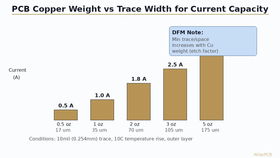
- Current capacity: A 10mil (0.25mm) trace carries ~1A with 10°C rise
- Cost: Baseline — this is the default copper weight
2 oz (70 um)
- Use case: Power electronics, LED drivers, motor controllers
- Minimum trace width: 4-5 mil (wider than 1oz due to etching limitations)
- Current capacity: Roughly doubles the capacity of 1oz for the same trace width
- Cost: ~15-25% more than 1oz
3 oz (105 um)
- Use case: High-current applications, industrial power supplies
- Minimum trace width: 5-6 mil
- Cost: ~30-50% more than 1oz
- Note: Etching precision decreases; trace edges become less defined
Heavy Copper PCB (4oz and Above)
Heavy copper PCBs use 4oz or more copper per layer. Some extreme applications use up to 20oz copper. These boards require specialized manufacturing processes.
Manufacturing Differences
- Etching challenges: Thick copper requires longer etching times, leading to more lateral etching (undercut). Trace widths must be wider to compensate.
- Plating uniformity: Achieving uniform plating in holes becomes difficult with thick copper.
- Lamination pressure: Higher pressure needed to bond thick copper to the substrate.
- Registration: Layer-to-layer alignment tolerances are larger.
Heavy Copper Design Rules
| Copper Weight | Min Trace Width | Min Spacing | Min Annular Ring |
|---|---|---|---|
| 4 oz | 8 mil (0.2mm) | 8 mil | 10 mil |
| 6 oz | 10 mil (0.25mm) | 10 mil | 12 mil |
| 10 oz | 14 mil (0.35mm) | 14 mil | 15 mil |
| 20 oz | 24 mil (0.6mm) | 24 mil | 20 mil |
Applications
- EV/HEV power electronics: Battery management, motor drives, DC-DC converters
- Power supplies: Server power, telecom rectifiers, industrial UPS
- Welding equipment: High-current control boards
- Military power systems: Ruggedized power distribution
- Planar transformers: PCB-integrated magnetics using heavy copper windings
Current Carrying Capacity
The IPC-2152 standard provides the most accurate guidance for trace current capacity. Key factors:
External (Outer) Layer Traces — 1oz Copper, 10°C Rise
| Trace Width | Max Current |
|---|---|
| 5 mil (0.13mm) | 0.5A |
| 10 mil (0.25mm) | 1.0A |
| 20 mil (0.5mm) | 1.7A |
| 50 mil (1.27mm) | 3.5A |
| 100 mil (2.54mm) | 6.0A |
| 200 mil (5.08mm) | 10.0A |
Effect of Copper Weight on Current Capacity
For the same trace width (20 mil / 0.5mm) and 10°C temperature rise:
| Copper Weight | Max Current | Relative Capacity |
|---|---|---|
| 0.5 oz | 1.1A | 65% |
| 1 oz | 1.7A | 100% (baseline) |
| 2 oz | 2.8A | 165% |
| 3 oz | 3.8A | 224% |
| 4 oz | 4.7A | 276% |
Key insight: Doubling copper weight does NOT double current capacity. The relationship is approximately: I ∝ (copper area)^0.725
Impact on Board Thickness
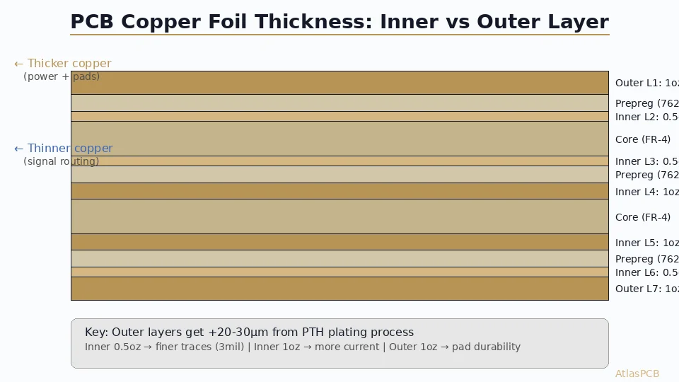
Copper weight directly affects total board thickness. For a standard 4-layer board:
| Copper Weight | Approx Board Thickness |
|---|---|
| 0.5 oz all layers | 1.2mm |
| 1 oz all layers | 1.6mm (standard) |
| 2 oz all layers | 2.0mm |
| 2 oz outer + 1 oz inner | 1.8mm |
| 3 oz outer + 1 oz inner | 2.0mm |
Custom stackups can maintain 1.6mm board thickness with heavier copper by adjusting prepreg and core thicknesses.
Thermal Considerations
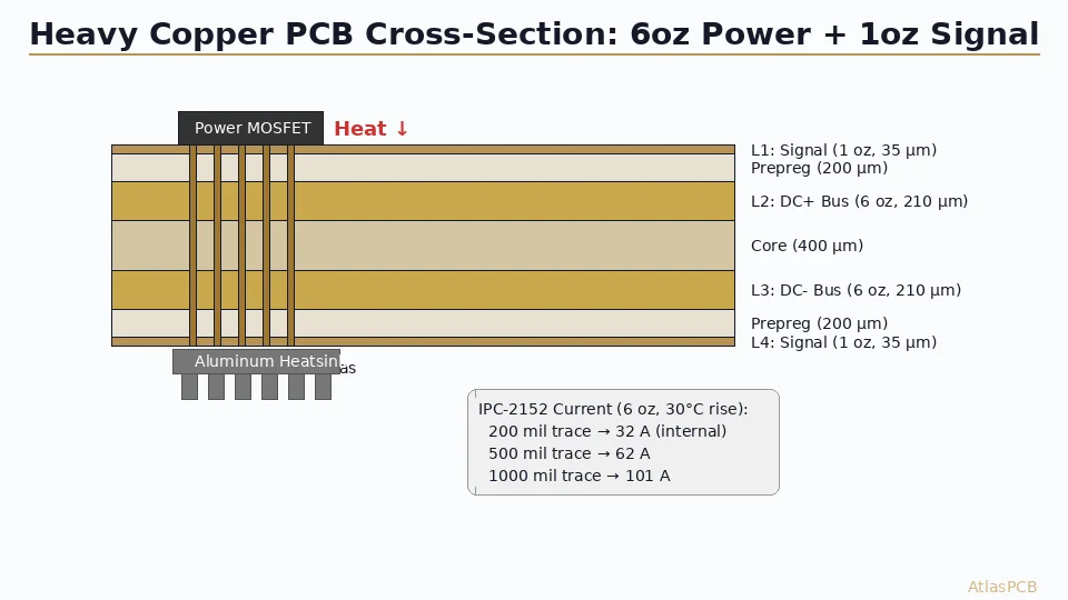
Copper is an excellent thermal conductor (385 W/m·K). Heavier copper improves:
- Heat spreading: Wider, thicker traces spread heat away from hot components
- Thermal vias: Heavier copper in via barrels improves vertical heat transfer
- Copper pour areas: Large copper fills act as heat sinks
Thermal Resistance Comparison
For a 10mm x 10mm copper area:
| Copper Weight | Thermal Resistance (°C/W) |
|---|---|
| 1 oz | ~90 |
| 2 oz | ~45 |
| 3 oz | ~30 |
Cost and Lead Time Impact
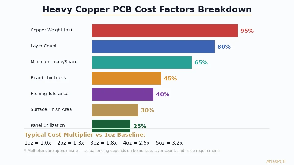
| Copper Weight | Cost Premium | Lead Time Impact |
|---|---|---|
| 0.5 oz | -5 to 0% | None |
| 1 oz | Baseline | Baseline |
| 2 oz | +15-25% | +1-2 days |
| 3 oz | +30-50% | +2-3 days |
| 4-6 oz | +50-100% | +3-5 days |
| 10+ oz | +100-200% | +5-10 days |
Conclusion
For most designs, 1oz copper is the default choice. Move to 2oz when you need more current capacity or better thermal performance. Consider 3oz+ only for dedicated power designs. Heavy copper (4oz+) is a specialized capability for high-power applications where the extra cost is justified by the performance requirements. Always consult your PCB manufacturer for their specific heavy copper capabilities and design rules.
About AtlasPCB — We specialize in complex PCB manufacturing for HDI, RF, and high-reliability applications. Explore our heavy copper PCB manufacturing . Every order includes free engineering review. Get your quote.
Reviewed by AtlasPCB Engineering Team — IPC-certified manufacturing specialists with 15+ years of production experience in HDI, RF, and high-reliability PCB fabrication. Content based on factory floor data and real customer design reviews.
Frequently Asked Questions
What does 1oz copper mean on a PCB?
When do I need heavy copper PCB?
- copper weight
- pcb thickness
- heavy copper
- current capacity