· Marcus Lin · Engineering · 7 min read
PCB Copper Foil Types
Understand the differences between electrodeposited (ED) and rolled annealed (RA) copper foil for PCB fabrication. Learn how grain structure, surface roughness, and ductility affect signal loss, flex reliability, and manufacturing cost.
Quick Answer
Electrodeposited (ED) copper foil has columnar grain structure and rougher surface, making it cheaper and providing excellent adhesion to substrates but with higher signal loss at high frequencies and poor flex fatigue resistance. Rolled annealed (RA) copper foil has elongated horizontal grains, ultra-smooth surfaces (Rz < 2 µm), and superior ductility — making it the mandatory choice for flex/rigid-flex circuits and preferred for RF applications above 5 GHz where insertion loss must be minimized.
The Role of Copper Foil in PCB Performance
Copper foil is the foundation of every PCB circuit — yet engineers often specify only the weight (thickness) while overlooking the foil type. This oversight can lead to:
- Unexpected insertion loss in high-speed channels
- Premature fatigue failure in flex circuits
- Impedance variation beyond tolerance
- Adhesion problems during fabrication
Two fundamentally different manufacturing processes produce copper foil for PCBs: electrodeposition (ED) and rolling + annealing (RA). Each creates distinct grain structures with dramatically different electrical, mechanical, and thermal properties.
This guide explains the engineering differences and helps you specify the right foil type for your application.
Electrodeposited (ED) Copper Foil
Manufacturing Process
ED foil is produced by electroplating copper from a copper sulfate solution onto a slowly rotating titanium drum:
- Copper ions deposit on the drum cathode surface
- The thin copper sheet is continuously peeled off as the drum rotates
- The foil passes through treatment baths for surface roughening, barrier layer, and silane coupling agent
Key process characteristics:
- Deposition rate: 1-3 µm/minute
- Drum side (smooth): Rz 1-3 µm
- Matte/bath side (rough): Rz 3-8 µm (standard), 1.5-4 µm (HVLP/RTF)
- Thickness range: 5 µm (¼ oz) to 210 µm (6 oz)
- Production speed: 5-15 m/min
Grain Structure
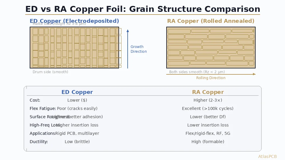
ED foil has columnar grain structure — crystals grow perpendicular to the drum surface like tiny pillars. This creates:
- Anisotropic mechanical properties (strong in-plane, weak across grain boundaries)
- Natural surface roughness on the bath/matte side
- Grain boundaries aligned perpendicular to the foil surface — creating easy crack propagation paths during bending
Surface Treatment Options
| Treatment | Roughness (Rz) | Trade Name Examples | Application |
|---|---|---|---|
| Standard | 5-8 µm | STD, S-bond | Multilayer rigid PCB |
| Low Profile (LP) | 3-5 µm | MLS, LP | High-speed digital |
| Very Low Profile (VLP) | 2-3.5 µm | VLP, TWLS | 10+ Gbps channels |
| Hyper Very Low Profile (HVLP) | 1.5-2.5 µm | SP, HVLP, RTF | 25+ Gbps, mmWave |
The rougher treatments provide better adhesion (higher peel strength) at the cost of increased signal loss. This is the fundamental trade-off in high-speed PCB material selection.
ED Foil Applications
- Standard multilayer rigid PCBs (most of global PCB production)
- Power electronics (heavy copper 3-6 oz)
- Automotive rigid boards (cost-sensitive, high volume)
- Digital designs < 5 GHz where loss budget is comfortable
- Any application where the board won’t be flexed
Rolled Annealed (RA) Copper Foil
Manufacturing Process
RA foil starts with a thick copper ingot that undergoes multiple rolling passes followed by thermal annealing:
- Cast copper ingot (200-300 mm thick)
- Hot rolling to ~5 mm
- Multiple cold rolling passes (reduction ratio 90-99%)
- Intermediate annealing (400-600°C) to restore ductility
- Final cold rolling to target thickness
- Final annealing to achieve desired temper (soft, half-hard, etc.)
- Surface treatment (minimal roughening needed due to natural smoothness)
Key process characteristics:
- Both surfaces equally smooth: Rz < 2 µm
- Grain structure: elongated, pancake-shaped, oriented parallel to the surface
- Superior purity control possible (99.99%+ Cu)
- Thickness range: 9 µm (⅓ oz) to 35 µm (1 oz) — thicker is possible but expensive
Grain Structure
RA foil has elongated horizontal grain structure — flattened by the rolling process and recrystallized by annealing into large, flat grains oriented parallel to the foil surface. This creates:
- Isotropic in-plane properties (similar strength in all directions parallel to surface)
- Excellent resistance to flex fatigue (cracks can’t easily propagate along the grain boundaries)
- Naturally smooth surfaces on both sides
- Higher ductility (elongation 15-25% vs 5-12% for ED)
RA Foil Variants
| Variant | Annealing | Grain Size | Flex Cycles | Application |
|---|---|---|---|---|
| RA (standard) | Standard | Medium | > 100,000 | Static flex, rigid-flex |
| HA (Hyper-Annealed) | Extended | Large | > 200,000 | Dynamic flex (hinges) |
| RA-HTE | Partial | Medium-small | > 50,000 | Moderate flex, better peel |

Need Flex or High-Frequency PCBs?
AtlasPCB manufactures flex, rigid-flex, and RF boards with proper RA copper foil specification and low-loss laminate selection.
Get a Quote →Signal Loss: The Roughness-Frequency Relationship
Skin Effect and Surface Roughness
At high frequencies, current concentrates in a thin layer at the conductor surface (skin effect). The skin depth (δ) decreases with frequency:
$$\delta = \sqrt{\frac{\rho}{\pi f \mu_0}} = \frac{66.1}{\sqrt{f_{GHz}}} \quad \text{µm (for copper)}$$
| Frequency | Skin Depth | Relevant Roughness |
|---|---|---|
| 100 MHz | 6.6 µm | Most roughness is below skin depth — minimal impact |
| 1 GHz | 2.1 µm | Roughness begins to matter (std ED: Rz 5-8 µm) |
| 5 GHz | 0.93 µm | Roughness significantly increases loss |
| 10 GHz | 0.66 µm | Surface profile dominates conductor loss |
| 28 GHz | 0.39 µm | Only ultra-smooth foil acceptable |
Hammerstad-Jensen Roughness Model
The increase in conductor loss due to surface roughness is modeled by:
$$K_{SR} = 1 + \frac{2}{\pi} \arctan\left(1.4 \left(\frac{R_q}{\delta}\right)^2\right)$$
Where Rq is the RMS surface roughness (approximately Rz/4 for typical profiles).
Practical loss increase at 10 GHz:
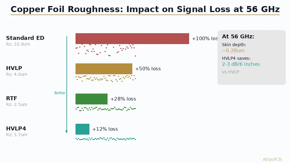
- Standard ED (Rz = 6 µm): K_SR ≈ 1.95 (95% increase over smooth copper)
- HVLP ED (Rz = 2 µm): K_SR ≈ 1.55 (55% increase)
- RA foil (Rz = 1.2 µm): K_SR ≈ 1.32 (32% increase)
- Theoretical smooth: K_SR = 1.00 (baseline)
Insertion Loss Comparison (5-inch 50Ω trace, 10 GHz)
| Foil Type | Conductor Loss | % vs Smooth | Channel Impact |
|---|---|---|---|
| Standard ED (Rz 6 µm) | 0.62 dB/inch | +95% | 3.1 dB extra over smooth |
| HVLP ED (Rz 2 µm) | 0.49 dB/inch | +55% | 2.45 dB extra |
| RA (Rz 1.2 µm) | 0.42 dB/inch | +32% | 2.1 dB extra |
| Theoretical smooth | 0.32 dB/inch | Baseline | — |
For 25+ Gbps designs, the difference between standard ED and RA foil can mean the difference between passing and failing channel compliance.
Flex Fatigue: Mechanical Performance
Failure Mechanism in ED vs RA
ED foil failure mode: Columnar grains create grain boundaries perpendicular to the surface. Under bending stress, cracks initiate at the rough surface and propagate straight down along the vertical grain boundaries — requiring minimal energy to traverse the full foil thickness.
RA foil failure mode: Elongated horizontal grains force any crack to repeatedly change direction, crossing grain boundaries at oblique angles. This crack-deflection mechanism absorbs far more energy, resulting in 10-20× greater fatigue life.
Flex Cycle Data (IPC-TM-650, Method 2.4.3)
| Foil Type | Thickness | Bend Radius | Cycles to Failure |
|---|---|---|---|
| ED Standard | 18 µm (½ oz) | 1.5 mm | 5,000-10,000 |
| ED Standard | 35 µm (1 oz) | 1.5 mm | 2,000-5,000 |
| RA Standard | 18 µm (½ oz) | 1.5 mm | 100,000-200,000 |
| RA Standard | 35 µm (1 oz) | 1.5 mm | 50,000-100,000 |
| HA (Hyper-Annealed) | 18 µm | 1.5 mm | > 200,000 |
For flex and rigid-flex PCB designs, RA foil is not optional — it’s the only technically viable choice for any zone that experiences repeated bending.
Static vs Dynamic Flex Applications
- Static flex (bent once during assembly, then stays): RA standard is sufficient
- Dynamic flex (continuous bending in service — laptop hinges, wearables): HA (hyper-annealed) foil required
- Rigid sections of rigid-flex: ED foil acceptable (cost optimization)
Cost and Availability
Price Comparison
| Foil Type | Relative Cost | Supply Chain |
|---|---|---|
| Standard ED | 1.0× (baseline) | Abundant, many suppliers |
| HVLP/RTF ED | 1.3-1.5× | Good availability |
| RA Standard | 2.0-3.0× | Limited suppliers (Mitsui, Fukuda, JX) |
| HA (Hyper-Annealed) | 2.5-4.0× | Specialized, longer lead time |
The cost premium of RA foil is justified when:
- Flex reliability requirements demand it (no alternative)
- High-frequency loss savings eliminate the need for a more expensive laminate
- The total board cost is dominated by other factors (complex stackup, fine features)
Major Foil Manufacturers
- Mitsui Mining & Smelting: MicroThin RA, TQ-VLP (ED)
- JX Nippon Mining: BHFX (RA), GTS-MP (HVLP ED)
- Fukuda Metal Foil: CF-T9 (RA), CF-H9M (HVLP ED)
- Circuit Foil Luxembourg: RTF-II (HVLP ED), STAR (RA)
- Nan Ya Plastics: Various ED profiles
Specification Guidelines for Engineers
When to Specify RA Foil
- All flex zone layers in flex/rigid-flex constructions
- RF/microwave circuits above 5 GHz on PTFE or LCP substrates
- 25+ Gbps SerDes channels where conductor loss budget is tight
- Wearable and implantable medical devices (dynamic flex + biocompatibility)
When ED (HVLP/RTF) is Sufficient
- Rigid-only boards at 5-25 GHz (good balance of cost vs performance)
- PCIe Gen5/Gen6 channels with adequate loss margin
- High-layer-count server boards where cost matters
- Automotive ADAS radar modules (28 GHz, but short trace lengths)
Stackup Notes
In your fabrication drawing, specify:
Layer 1 (Top):     ED HVLP, 1 oz (35 µm), Rz ≤ 2.5 µm
Layer 2 (GND):     ED Standard, ½ oz (18 µm)
...
Flex Layer 7:      RA, ½ oz (18 µm), Rz ≤ 1.5 µm
Flex Layer 8:      RA, ½ oz (18 µm), Rz ≤ 1.5 µm
Always specify both the foil type AND the maximum roughness requirement to avoid substitution.
Further Reading
- Copper Roughness and High-Speed Signal Loss
- Rigid-Flex PCB Design Guide
- RF PCB Material Selection
- High-Speed Material Dk/Df Comparison
Designing with RA or HVLP copper foil? AtlasPCB stocks leading RA foil brands and HVLP ED laminates for flex, rigid-flex, and high-frequency applications. Request a quote with your stackup requirements.
About AtlasPCB — We specialize in complex PCB manufacturing for HDI, RF, and high-reliability applications. Explore our RF and high-frequency PCB services, or get an rigid-flex PCB manufacturing . Every order includes free engineering review. Get your quote.
Reviewed by AtlasPCB Engineering Team — IPC-certified manufacturing specialists with 15+ years of production experience in HDI, RF, and high-reliability PCB fabrication. Content based on factory floor data and real customer design reviews.
Frequently Asked Questions
Why does copper foil surface roughness affect high-frequency signal loss?
How many flex cycles can RA copper foil survive compared to ED?
Can I use ED foil for rigid-flex PCBs?
- copper-foil
- ed-copper
- ra-copper
- flex-pcb
- high-frequency
- signal-loss
- rf-materials
- manufacturing