· Priya Nair · Engineering · 8 min read
IPC-A-610 Class 3 Inspection
Complete guide to IPC-A-610 Class 3 inspection criteria for solder joints, component placement, cleanliness, and board condition. Learn the specific accept/reject criteria that separate high-reliability assemblies from standard products.
Quick Answer
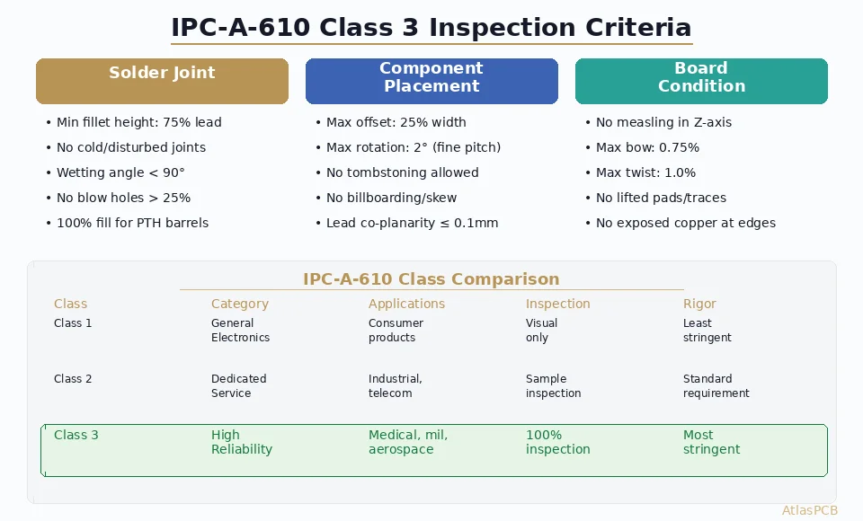
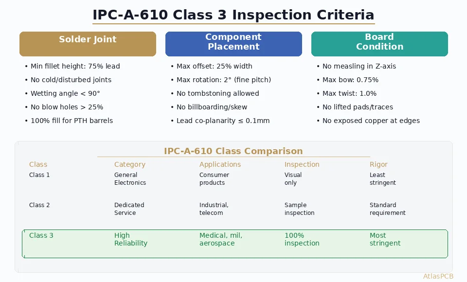
IPC-A-610 Class 3 is the highest workmanship standard for electronic assemblies, required for medical devices, aerospace, and military applications where failure is not acceptable. It mandates 100% visual inspection, tighter solder joint acceptance criteria (minimum 75% fillet height, no voiding above 25% in BGA joints), stricter component placement tolerances (max 25% offset for chip components), and zero tolerance for defects like measling, lifted pads, or damaged plating.
What IPC-A-610 Actually Covers
IPC-A-610, titled “Acceptability of Electronic Assemblies,” is the most widely used standard for judging the quality of assembled PCBs. Now in its ninth revision (IPC-A-610H, released 2024), it provides detailed visual criteria — with hundreds of photographs — showing what constitutes acceptable, process indicator, and defect conditions for every aspect of a populated circuit board.
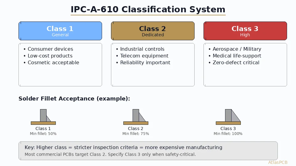
The standard organizes criteria into three performance classes:
- Class 1: General Electronic Products (consumer disposable, short-life)
- Class 2: Dedicated Service Electronic Products (industrial, commercial)
- Class 3: High-Reliability Electronic Products (medical, military, aerospace)
This article focuses on Class 3 requirements — the most stringent level, where every solder joint, every component placement, and every board surface must meet explicit accept/reject criteria.
Why Class 3 Exists
Class 3 was designed for applications where electronic failure has consequences beyond inconvenience:
- Medical devices: A solder joint failure in a pacemaker or ventilator can be fatal
- Aerospace/avionics: An assembly defect in a flight control system can cause aircraft loss
- Military systems: Equipment must survive extreme environments and extended service life
- Spacecraft: No repair possible once deployed — every joint must be right the first time
The core philosophy: continuous, reliable operation is mandatory, and there is no acceptable level of defect. Conditions that Class 2 accepts as “process indicators” (not ideal but acceptable) are classified as “defects” in Class 3, requiring rework or rejection.
Solder Joint Criteria — The Heart of Class 3
Through-Hole (PTH) Solder Joints
Through-hole solder joints in Class 3 assemblies must demonstrate:
Fillet requirements:
- Minimum solder fill: 75% of barrel height (Class 2 requires only 50%)
- Solder fillet must wet to the lead and the pad on both top and bottom sides
- Fillet must be visible and continuous — no gaps, cracks, or non-wetting
Wetting angle:
- Contact angle between solder and pad must be < 90° (good wetting)
- Smooth, concave fillet profile indicates proper intermetallic formation
- Convex (balled) solder profiles indicate non-wetting — defect in all classes
Barrel fill:
- For Class 3 PTH: solder must be visible in the barrel and show evidence of capillary fill
- Pin-in-paste (intrusive reflow) joints must meet the same barrel fill criteria as wave-soldered joints
- No voiding visible at top or bottom pad surfaces
SMT Solder Joints — Chip Components (0201–2512)
Surface mount chip component solder joints are judged by six criteria:
- Side overhang (A): Maximum 25% of component width (Class 2 allows 50%)
- End overhang (B): Component metallization must not extend beyond the pad
- Side fillet height (C): Minimum solder wetting to component side metallization
- End fillet height (D): Minimum 25% of component height or 0.5 mm, whichever is less
- Heel fillet (E): Solder must wet continuously from pad to component termination
- Fillet width (F): Equal to or greater than component termination width
Class 3 specifics:
- No solder balls or splatter within 0.13 mm of uncoated conductors
- Maximum 1 void per joint (visible without magnification)
- No disturbed or cold joints (grainy, dull appearance)
- No dewetting (solder pulls away from pad surface)
BGA Solder Joints
BGA inspection in Class 3 requires X-ray examination for every board (100% inspection):
X-ray criteria:
- Voiding < 25% of ball area (measured from X-ray image)
- No head-on-pillow (HoP) defects — ball must show complete merge with paste deposit
- No bridging between adjacent balls
- Ball diameter uniformity: within 20% of nominal across the array
- No missing balls (100% ball count verification)
Cross-section criteria (periodic validation):
- Intermetallic compound (IMC) thickness: 1–3 μm (too thin = no bond, too thick = brittle)
- No Kirkendall voids at the IMC interface
- Crack-free solder/pad interface after thermal cycling coupon tests
Component Placement Tolerances
Chip Components (Resistors, Capacitors)
| Criteria | Class 2 | Class 3 |
|---|---|---|
| Max lateral offset | 50% of W or pad, lesser | 25% of W or pad, lesser |
| Max end joint width reduction | 50% | 25% |
| End overhang beyond pad | 50% of termination | 25% of termination |
| Rotation (rectangular) | Not touching adjacent pad | Not touching adjacent pad |
| [Tombstoning]/blog/pcb-tombstoning-causes-prevention-dfm/) | Defect | Defect |
| Billboarding | Process indicator | Defect |
| Component shift (after reflow) | — | < 25% of shortest dim |
Fine-Pitch ICs (QFP, QFN)
Fine-pitch components (≤ 0.5 mm pitch) have additional constraints in Class 3:
- Lead-to-pad offset: maximum 25% of lead width
- Heel fillet mandatory on all leads (no exceptions)
- Lead co-planarity: ≤ 0.10 mm (measured before placement; leads exceeding this must be reformed)
- Solder bridging between any two leads: defect requiring removal and re-inspection
Odd-Form Components (Connectors, Switches, Transformers)
- All mechanical fasteners must be secure and properly seated
- Connector pins must show full wetting in plated through-holes (75% barrel fill minimum)
- Stand-off height between component body and board: per manufacturer specification ±10%
- Press-fit pins must show proper hole deformation without barrel cracking
Need IPC Class 3 Assembly and Inspection?
AtlasPCB partners with certified EMS facilities for Class 3 PCBA — full AOI, X-ray, and first-article inspection per IPC-A-610H.
Request Class 3 PCBA Quote →Board and Assembly Condition
Cleanliness (IPC-A-610 Section 10)
Class 3 cleanliness requirements go beyond visual inspection:
Ionic contamination:
- Maximum 1.56 μg NaCl equivalent per cm² (ROSE test)
- For no-clean processes: validate with Surface Insulation Resistance (SIR) testing
- Ion chromatography for Class 3 when flux residue is present
Particulate contamination:
- No loose solder balls on the assembly
- No foreign material under components (especially under BGAs and QFNs)
- No conductive particles near uncoated conductors
Flux residue (no-clean process):
- Residue must not bridge between conductors
- No white/crystalline residue (indicates incomplete reflow or wrong flux type)
- Residue must not interfere with test probe contact or conformal coating adhesion
Board Damage Criteria
| Condition | Class 2 | Class 3 |
|---|---|---|
| Measling (white spots) | Accept if ≤ 4 spots per cm² | Defect if in Z-axis direction |
| Crazing (micro-cracks) | Accept if doesn’t cross conductors | Defect |
| [Delamination]/blog/what-causes-pcb-delamination/) | Defect if > 1% of area | Defect — zero tolerance |
| Lifted pad | Defect if > 1 pad lifted | Defect — zero tolerance |
| Bow | ≤ 1.5% | ≤ 0.75% |
| Twist | ≤ 1.5% | ≤ 1.0% |
| Exposed copper at board edge | Accept if < 0.8 mm from edge | Defect |
| Nick/scratch in conductor | Accept if < 20% of width removed | Accept if < 10% of width |
Conformal Coating (IPC-A-610 Section 12)
When [conformal coating]/blog/conformal-coating-pcb/) is specified for Class 3:
- Coverage must be complete and uniform on all specified areas
- No bubbles > 0.5 mm diameter
- No de-wetting or fisheyes
- No coating on mating connectors, test points, or designated keep-out areas
- Thickness must be within specification for the coating type (typically 25–75 μm for acrylic, 50–130 μm for urethane)
Inspection Methods for Class 3
Visual Inspection Requirements
Class 3 demands 100% inspection of all solder joints and component placements. This means:
- Every joint on every board is examined
- Minimum magnification: 4× for general inspection, 10× for fine-pitch (< 0.5 mm)
- Lighting: uniform, shadow-free illumination at 1000–3000 lux
- Inspector certification: IPC-A-610 CIS (Certified IPC Specialist) or equivalent
Automated Optical Inspection (AOI)
[AOI systems]/blog/aoi-spi-inspection-pcb-assembly-quality-control/) complement but do not replace human inspection in Class 3:
- AOI catches 85–95% of defects automatically (placement, bridging, missing components)
- Human inspector verifies AOI results and inspects conditions AOI cannot judge (wetting quality, joint appearance)
- AOI programming must be validated against golden boards with known defects
X-Ray Inspection
Mandatory for Class 3 when hidden joints exist:
- BGA, QFN, LGA: 100% X-ray inspection
- Pin-in-paste through-hole: X-ray to verify barrel fill when visual access is blocked
- Reworked areas: X-ray to verify rework quality
First Article Inspection (FAI)
Before production begins, the first complete assembly undergoes detailed inspection:
- All dimensions verified against IPC-A-610 criteria
- Cross-section of representative solder joints (destructive testing)
- Pull-test or shear-test of selected components
- Documentation of all inspection results for the production file
Common Class 3 Failures and Root Causes
Insufficient Solder Fill (PTH)
Root causes:
- Paste volume too low for pin-in-paste process
- Wave solder temperature too low or contact time too short
- Barrel aspect ratio too high (> 8:1 for standard, > 5:1 for Class 3)
- Poor plating quality in the [PCB barrel]/blog/pcb-plated-through-hole-reliability/)
Prevention:
- Increase paste volume (larger stencil apertures for PTH pads)
- Verify via/hole plating quality per IPC-6012 before assembly
- Use nitrogen-assist wave soldering for improved fill
Tombstoning
Root causes:
- Asymmetric pad design or solder paste deposits
- Reflow profile imbalance (one end reaches liquidus before the other)
- Component too light (small chip resistors/capacitors)
Prevention:
- Follow [DFM guidelines for tombstone prevention]/blog/pcb-tombstoning-causes-prevention-dfm/)
- Ensure symmetric pad geometry and [stencil aperture design]/blog/pcb-solder-paste-stencil-design/)
- Optimize reflow profile for thermal uniformity
BGA Voiding > 25%
Root causes:
- Flux outgassing during reflow
- Moisture absorption in PCB or BGA package
- Inadequate reflow profile (too fast ramp → trapped volatiles)
Prevention:
- Bake boards and components per [IPC-J-STD-033 moisture sensitivity guidelines]/blog/pcb-moisture-sensitivity-baking/)
- Use vacuum-assist reflow for critical BGA assemblies
- Optimize soak zone temperature and duration
The Relationship Between IPC-A-610 and Other Standards
IPC-A-610 works within an ecosystem of interconnected standards:
- IPC-J-STD-001 (Requirements for Soldered Electrical and Electronic Assemblies): Prescriptive process standard — tells you how to solder. IPC-A-610 is the acceptance standard — tells you what’s acceptable.
- IPC-A-600 (Acceptability of Printed Boards): Bare board acceptance before assembly. [IPC-A-600 Class 3 criteria]/blog/ipc-a-600-class-2-vs-class-3-pcb-acceptability/) feed into A-610 Class 3 assembly.
- IPC-6012 (Qualification and Performance Specification for Rigid PCBs): Defines board performance requirements including [IPC standards and PCB classes]/blog/ipc-standards-pcb-classes/).
- IPC-7711/7721 (Rework, Modification, and Repair): Defines acceptable rework procedures. Class 3 limits the number and type of reworks allowed.
For a complete Class 3 program, specify: IPC-6012 Class 3 (bare board) + IPC-J-STD-001 Class 3 (process) + IPC-A-610 Class 3 (acceptance).
Implementing Class 3 in Your Organization
Training Requirements
All personnel involved in Class 3 production must be trained:
- Operators: IPC-A-610 CIS certification (Certified IPC Specialist)
- Inspectors: IPC-A-610 CIS with hands-on inspection experience
- Engineers: Understanding of all relevant IPC standards
- Re-certification every 2 years
Process Control
Class 3 requires documented process control for every operation:
- Solder paste printing: SPI verification with statistical process control
- [Reflow profiling]/blog/reflow-soldering-profile-optimization-lead-free-pcb-assembly/): Validated profile for each board design, re-validated for any change
- Wave soldering: Daily parameter verification (temperature, speed, flux density)
- Rework: Limited to qualified operators with documented procedures
Documentation
Every Class 3 assembly requires a complete quality record:
- Incoming inspection results (PCB, components)
- SPI data for each panel
- AOI results with disposition
- X-ray results for hidden joints
- Manual inspection results
- Any rework documentation (what, where, who, how)
- Final acceptance sign-off
Further Reading
- [IPC-A-600 Class 2 vs Class 3 PCB Acceptability]/blog/ipc-a-600-class-2-vs-class-3-pcb-acceptability/) — Bare board acceptance criteria
- [AOI and SPI Inspection for PCB Assembly Quality Control]/blog/aoi-spi-inspection-pcb-assembly-quality-control/) — Automated inspection technology
- [Common PCB Defects and Prevention]/blog/common-pcb-defects-prevention/) — Defect catalog with root causes
- [Medical Device PCB Standards]/blog/medical-device-pcb-standards/) — Regulatory requirements for medical electronics
- [IPC Standards and PCB Classes Explained]/blog/ipc-standards-pcb-classes/) — Overview of the IPC standard ecosystem
Building a high-reliability product that requires IPC-A-610 Class 3? AtlasPCB manufactures bare boards to IPC-6012 Class 3 and partners with certified EMS providers for Class 3 assembly. Start your Class 3 project →
About AtlasPCB — We specialize in complex PCB manufacturing for HDI, RF, and high-reliability applications. Explore our full PCB manufacturing capabilities . Every order includes free engineering review. Get your quote.
Reviewed by AtlasPCB Engineering Team — IPC-certified manufacturing specialists with 15+ years of production experience in HDI, RF, and high-reliability PCB fabrication. Content based on factory floor data and real customer design reviews.
Frequently Asked Questions
What is the difference between IPC-A-610 Class 2 and Class 3?
Does IPC-A-610 cover bare PCB quality or only assembled boards?
Is IPC-A-610 Class 3 required for all medical devices?
- ipc-a-610
- inspection
- quality-control
- solder-joint
- class-3
- high-reliability
- workmanship
- pcba
- medical-pcb
- aerospace