· Sophia Reyes · Engineering · 7 min read
How to Specify PCB Copper Weight
Complete guide to specifying copper weight in PCB fabrication drawings. Covers current capacity calculations, etch factor constraints on trace width, inner vs outer layer differences, and cost implications from 0.5oz to 5oz copper.
Quick Answer
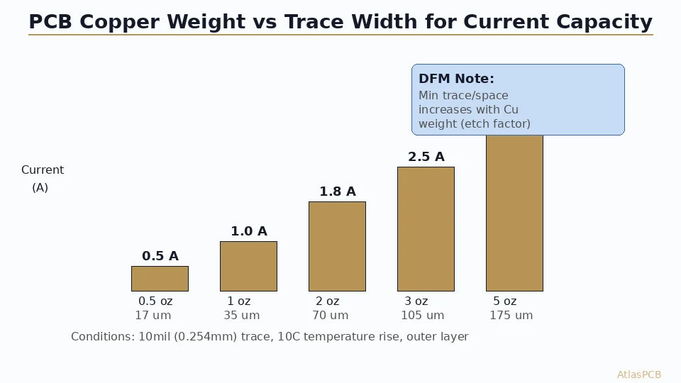
Specify copper weight based on required current capacity and minimum trace/space constraints. Standard 1oz (35um) copper carries approximately 1A per 10mil (0.254mm) trace at 10C rise on outer layers. For higher current, use 2oz (70um) copper but increase minimum trace/space from 4/4mil to 5/5mil due to etch factor. Inner layers carry 50% less current than outer layers at the same geometry due to reduced convective cooling.
Quick Reference: Copper Weight Selection
| Current Need (per trace) | Recommended Weight | Min Trace (outer) | Min Space | Typical Use |
|---|---|---|---|---|
| Under 0.5A | 0.5oz (17um) | 3/3 mil | 3 mil | Signal routing, RF |
| 0.5-1.5A | 1oz (35um) | 3/3 mil | 3 mil | General purpose |
| 1.5-3A | 2oz (70um) | 5/5 mil | 5 mil | Power, LED drivers |
| 3-5A | 3oz (105um) | 6/6 mil | 6 mil | Motor drives, power supply |
| 5-10A | 5oz (175um) | 8/8 mil | 8 mil | High-power, bus bars |
Note: Values assume 10C temperature rise on outer layers. Inner layers carry approximately 50% less at same geometry.
The Etch Factor Problem
This is the single most common DFM issue with heavy copper. Every PCB engineer needs to understand it.
When copper is etched, the etchant attacks sideways as well as downward. The ratio of vertical etch depth to lateral undercut is the “etch factor.” For standard chemistry:
- 1oz copper: Etch factor 3:1 to 4:1 (undercut ~9-12um per side)
- 2oz copper: Etch factor 2.5:1 to 3:1 (undercut ~23-28um per side)
- 3oz copper: Etch factor 2:1 to 2.5:1 (undercut ~42-53um per side)
- 5oz copper: Etch factor 1.5:1 to 2:1 (undercut ~88-117um per side)
What this means in practice:
A trace drawn as 5mil (127um) in your Gerber file, fabricated in 3oz copper, will have:
- Top width: 127um - 2 x 50um = ~27um (barely viable)
- Bottom width: 127um (at copper-substrate interface)
- Trapezoidal cross-section
This is why heavy copper demands wider minimum trace widths. Your CAD tool shows rectangular traces, but the fabricated result is trapezoidal.
Fabrication Compensation
Reputable fabricators (including AtlasPCB) apply etch compensation — we widen your traces in the photo tool by the expected undercut amount. But this only works if:
- Your traces are wide enough that compensation leaves a viable top width
- Your spaces are wide enough to remain clear after compensation widens adjacent traces
- You specify copper weight clearly so we know how much to compensate
Never design at minimum trace width for heavy copper without confirming with your fabricator.
DFM REVIEW
Heavy Copper Design? Submit for Manufacturability Check
Upload your Gerber files and stackup. We verify trace/space meets etch factor limits for your specified copper weight before production.
Upload Gerber Files ›
Current Capacity Calculations
The industry standard reference is IPC-2152 (supersedes the older IPC-2221 charts). Key variables:
- Trace width (the primary design knob)
- Copper thickness (your specified weight)
- Allowable temperature rise (typically 10C, 20C, or 30C above ambient)
- Layer position (outer vs inner — inner carries less due to poor heat dissipation)
Outer Layer Current Capacity (10C Rise)
| Trace Width | 0.5oz | 1oz | 2oz | 3oz | 5oz |
|---|---|---|---|---|---|
| 5 mil (0.127mm) | 0.3A | 0.5A | 0.8A | 1.1A | 1.6A |
| 10 mil (0.254mm) | 0.5A | 1.0A | 1.8A | 2.5A | 3.8A |
| 20 mil (0.508mm) | 0.9A | 1.7A | 3.0A | 4.2A | 6.5A |
| 50 mil (1.27mm) | 1.8A | 3.2A | 5.5A | 7.8A | 12A |
| 100 mil (2.54mm) | 3.0A | 5.5A | 9.5A | 13A | 20A |
Inner Layer Derating
Inner copper layers are sandwiched in laminate with poor thermal conductivity (~0.3 W/mK for FR-4). Apply these factors:
- Inner layer capacity = Outer capacity x 0.5 (for same 10C rise)
- Or equivalently, double the trace width for inner power planes
- Ground/power planes are exceptions — large copper pours dissipate effectively via thermal vias
Thermal Via Enhancement
For components with exposed thermal pads (QFNs, power MOSFETs), thermal vias connecting the pad to an inner ground plane can increase effective current capacity by 40-60%. AtlasPCB supports via-in-pad with conductive fill (VIPPO) for this application.
Specifying Copper Weight in Your Fab Drawing
Your fabrication drawing (or README/stackup document) must clearly state:
Required Information
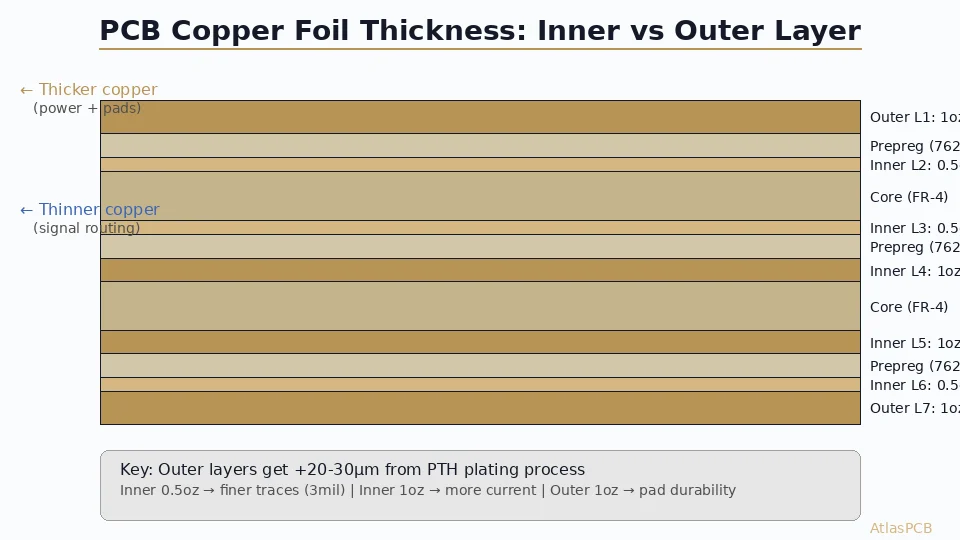
- Copper weight per layer — do not assume fabricator knows your intent
- Finished copper thickness vs starting copper — important distinction:
- Starting copper (base foil): What you order (e.g., 1oz = 35um)
- Finished copper (after plating): Adds ~20-25um from electroless + electrolytic plating on outer layers
- A “1oz finished” outer layer actually starts as ~0.5oz base foil + plating
- Whether inner layers include plating — inner layers typically stay at base foil weight (no additional plating unless via holes are plated)
Example Stackup Table (6-Layer, Mixed Copper)
| Layer | Function | Starting Cu | Finished Cu | Min Trace/Space |
|---|---|---|---|---|
| L1 | Signal + Power | 1oz (35um) | ~57um (with plating) | 4/4 mil |
| L2 | Ground Plane | 1oz (35um) | 35um | N/A (pour) |
| L3 | Signal | 0.5oz (17um) | 17um | 3/3 mil |
| L4 | Power Plane | 2oz (70um) | 70um | N/A (split pour) |
| L5 | Ground Plane | 1oz (35um) | 35um | N/A (pour) |
| L6 | Signal + Power | 1oz (35um) | ~57um (with plating) | 4/4 mil |
STACKUP ENGINEERING
Need a Custom Stackup with Mixed Copper Weights?
AtlasPCB engineers design impedance-controlled stackups with optimized copper weight per layer. Up to 30 layers, 5oz outer / 3oz inner.
Common Mistakes and How to Avoid Them
Mistake 1: Specifying 2oz Everywhere “Just in Case”
Engineers sometimes specify 2oz on all layers for current margin. The consequences:
- Inner signal layers lose fine-trace capability (5/5mil minimum vs 3/3mil)
- Board cost increases 10-20% for the extra copper
- Impedance matching becomes harder (wider traces for same impedance)
- Board weight increases (matters for aerospace/portable)
Fix: Use heavy copper only on power layers. Route signals on 0.5oz or 1oz layers.
Mistake 2: Ignoring Copper Balance
Unequal copper distribution between top/bottom or between inner layers causes board warpage during lamination. The copper on each side creates differential thermal expansion stress.
Rule of thumb: Keep copper fill percentage within 20% between paired layers (L1/L6, L2/L5, etc.). Use copper thieving patterns on sparse layers.
See our detailed guide on copper balancing techniques for quantitative analysis.
Mistake 3: Not Accounting for Plating Thickness on Outer Layers
If your impedance simulation uses 1oz (35um) for the outer layer trace thickness, your manufactured board will be wrong. Outer layers receive 20-25um additional plating during the PTH process. The actual trace thickness is 55-60um, which changes impedance by 3-8%.
Fix: Simulate with finished copper thickness. Ask your fabricator for their typical plating addition.
Mistake 4: Thermal Relief Pads Too Narrow for Heavy Copper
Thermal relief spokes connecting a pad to a power plane must be wide enough to carry current and survive etching:
- 1oz copper: 8mil spoke width minimum
- 2oz copper: 12mil spoke width minimum
- 3oz copper: 16mil spoke width minimum
Narrow spokes in heavy copper etch to nothing, leaving the pad electrically disconnected.
POWER ELECTRONICS
Heavy Copper PCBs for Power Conversion
Motor drives, power supplies, EV chargers -- AtlasPCB fabricates up to 5oz outer / 3oz inner copper with controlled impedance on signal layers.
Request Power Board Quote ›Cost Impact Summary
| Change | Cost Impact | When Worth It |
|---|---|---|
| 0.5oz → 1oz (outer) | +0% (standard) | Always default |
| 1oz → 2oz (outer) | +10-15% | Current >1.5A per trace |
| 2oz → 3oz (outer) | +20-30% | Current >3A, power boards |
| 3oz → 5oz (outer) | +40-60% | Current >5A, bus bar replacement |
| 1oz → 2oz (inner only) | +15-25% | Power plane needs |
| Mixed weights | +5-10% vs uniform heavy | Optimized cost/performance |
The most cost-effective approach for power-intensive designs: use 2oz outer + 1oz inner with wide power traces, rather than 3oz everywhere with narrow traces. You get equivalent current capacity at lower cost and better signal routing flexibility.
ATLASPCB
Upload Your Design for Copper Weight Optimization
Our engineers review your stackup, current requirements, and trace geometry to recommend the most cost-effective copper configuration.
Get Instant Quote ›
Related Reading:
About AtlasPCB — We specialize in complex PCB manufacturing for HDI, RF, and high-reliability applications. Explore our multilayer PCB fabrication up to 30 layers, or get an free engineering DFM review . Every order includes free engineering review. Get your quote.
Reviewed by AtlasPCB Engineering Team — IPC-certified manufacturing specialists with 15+ years of production experience in HDI, RF, and high-reliability PCB fabrication. Content based on factory floor data and real customer design reviews.
Frequently Asked Questions
What is the difference between 1oz and 2oz copper on a PCB?
Can I mix copper weights on different layers?
How does copper weight affect impedance control?
What is the maximum copper weight AtlasPCB supports?
- copper weight
- PCB design
- current capacity
- DFM
- stackup
- trace width
- power delivery