· Sophia Reyes · Engineering · 3 min read
How to Reduce PCB Crosstalk
Engineering guide to reducing PCB crosstalk. Covers near-end and far-end crosstalk mechanisms, 3W and 5W spacing rules, guard traces, stripline vs microstrip, stackup optimization, and simulation methodology for high-speed digital designs.
Quick Answer
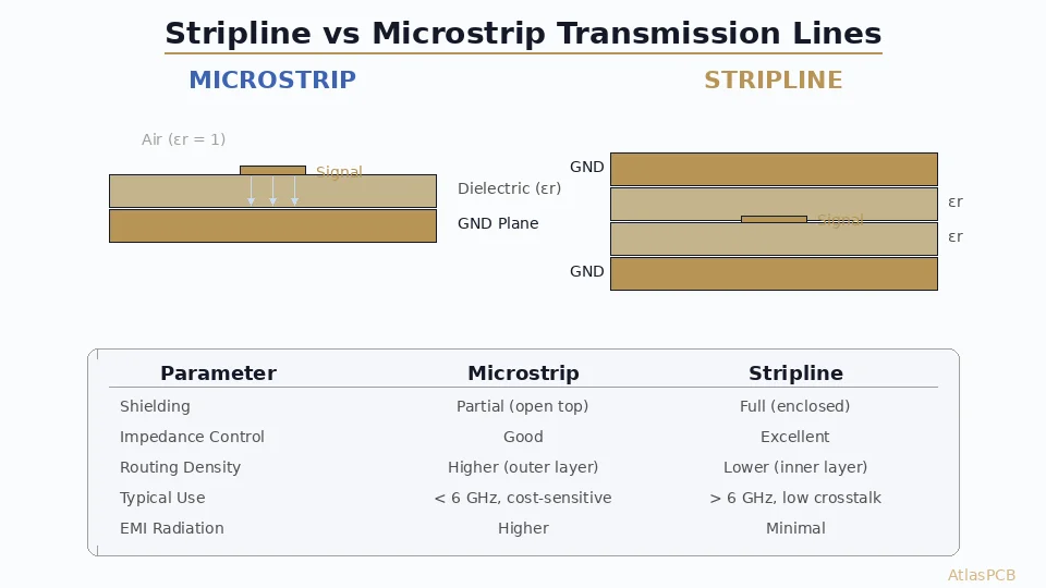
PCB crosstalk is reduced through four primary techniques: maintaining adequate trace spacing (3W rule for general signals, 5W for critical pairs where W is the trace width), using stripline routing instead of microstrip (10-15 dB less crosstalk due to shielding ground planes), implementing guard traces with via stitching between sensitive signals, and optimizing stackup with thin dielectric layers that tightly couple signals to their reference planes. Near-end crosstalk (NEXT) is the dominant concern in most digital designs, while far-end crosstalk (FEXT) becomes critical in long parallel runs exceeding 2 inches.
How to Reduce PCB Crosstalk: Spacing Rules & Layout Techniques
Crosstalk—the unwanted coupling of energy between adjacent signal traces—is one of the most common causes of signal integrity failures in high-speed PCB designs. A single crosstalk violation can corrupt data, cause bit errors, and fail compliance testing. The insidious nature of crosstalk is that it scales with frequency and can emerge late in the design cycle when layout changes are expensive.
This guide covers the physics of crosstalk, practical reduction techniques, and the design rules that prevent crosstalk from becoming a problem in the first place.
Understanding Crosstalk Mechanisms
Near-End Crosstalk (NEXT)
NEXT occurs at the near end (driving end) of the victim trace. It is caused by both capacitive and inductive coupling from the aggressor trace. Key characteristics:
- Amplitude is proportional to the rise time of the aggressor signal
- Saturates when the coupled length exceeds the critical length (Lc = rise_time × propagation_velocity / 2)
- Polarity: same as aggressor for microstrip, depends on geometry for stripline
Far-End Crosstalk (FEXT)
FEXT appears at the far end of the victim trace. In homogeneous media (stripline), FEXT theoretically cancels to zero. In practice:
- Microstrip FEXT is significant and proportional to coupled length
- Stripline FEXT is approximately 10-20× smaller than microstrip FEXT
- This is the strongest argument for routing critical signals as stripline
Crosstalk Reduction Techniques
Technique 1: Adequate Trace Spacing
The most effective and lowest-cost technique:
| Spacing Rule | Gap (for 4 mil trace) | Crosstalk Reduction | Application |
|---|---|---|---|
| 1W (edge-to-edge = width) | 4 mil gap | Baseline (-20 dB) | Minimum spacing |
| 2W (center-to-center) | 4 mil gap | -30 dB | General digital |
| 3W (center-to-center) | 8 mil gap | -40 dB | Standard high-speed |
| 5W (center-to-center) | 16 mil gap | -50 dB | Clocks, critical |
Technique 2: Stripline vs Microstrip Selection
Route crosstalk-sensitive signals on inner layers (stripline):
| Parameter | Microstrip | Stripline |
|---|---|---|
| NEXT | Higher | Lower |
| FEXT | Significant | Near zero (homogeneous) |
| Routing density | Higher (wider traces) | Lower |
| Impedance control | Affected by solder mask | More predictable |
Technique 3: Guard Traces
Guard traces between critical signals provide additional isolation:
- Must be grounded with vias every λ/10 at the highest frequency
- Typical via spacing: 100-200 mil for multi-GHz signals
- Provides additional 6-15 dB isolation when properly implemented
- Without via stitching, guard traces can worsen crosstalk
Technique 4: Stackup Optimization
Tighter coupling between signal and reference plane reduces crosstalk:
- Reduce dielectric thickness between signal and reference layers
- Use thin prepreg (2-3 mil) for signal-to-ground spacing
- Each 50% reduction in dielectric thickness reduces crosstalk by approximately 6 dB
See our [signal integrity PCB design guide]/blog/signal-integrity-pcb-design-guide/) and [PCB grounding techniques guide]/blog/pcb-grounding-techniques/) for comprehensive signal integrity strategies.
Design Rules Summary
| Signal Category | Min Spacing | Routing Layer | Guard Trace |
|---|---|---|---|
| Low-speed digital (<100 MHz) | 2W | Any | Not needed |
| DDR4/5 data | 3W | Stripline preferred | Optional |
| PCIe Gen 3/4 | 4W | Stripline | Recommended |
| PCIe Gen 5/6 | 5W | Stripline mandatory | Required |
| RF/microwave | 5W+ | Stripline | Required with via fence |
| Clocks | 5W | Stripline | Required |
Ready to optimize your high-speed layout? Upload your design for a free signal integrity review.
Further Reading
- [Signal Integrity in PCB Design]/blog/signal-integrity-pcb-design-guide/)
- [Differential Pair Routing: Rules & Common Mistakes]/blog/differential-pair-routing-pcb/)
- [PCB Grounding Techniques]/blog/pcb-grounding-techniques/)
About AtlasPCB — We specialize in complex PCB manufacturing for HDI, RF, and high-reliability applications. Explore our impedance-controlled PCB manufacturing, or get an Megtron 6 & 7 low-loss PCB manufacturing . Every order includes free engineering review. Get your quote.
Reviewed by AtlasPCB Engineering Team — IPC-certified manufacturing specialists with 15+ years of production experience in HDI, RF, and high-reliability PCB fabrication. Content based on factory floor data and real customer design reviews.
Frequently Asked Questions
What is the 3W rule for PCB crosstalk?
Is stripline or microstrip better for reducing crosstalk?
Do guard traces actually reduce crosstalk?
- signal-integrity
- crosstalk
- pcb-design
- high-speed