· Thomas Webb · Engineering · 8 min read
Heavy Copper PCB Cost Breakdown
Detailed cost analysis of heavy copper PCB fabrication covering 2oz through 5oz designs. Breaks down how copper weight, etching challenges, minimum trace/space, layer count, and board thickness affect pricing. Includes cost multipliers, optimization strategies, and when heavy copper makes financial sense vs alternative approaches.
Quick Answer
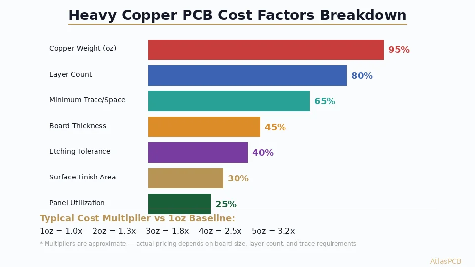
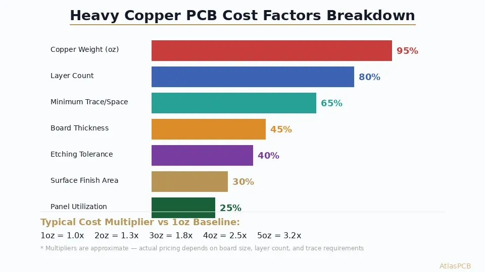
Heavy copper PCBs (2oz-5oz) cost 1.3x to 3.2x more than standard 1oz boards, with copper weight being the dominant cost driver (accounting for roughly 40-50% of the price premium). A 4-layer board with 3oz copper on outer layers typically costs $18-28/board at 100-piece quantity (100x100mm), compared to $8-12 for the same design in 1oz. The cost scales non-linearly because thicker copper requires wider trace/space (reducing routing density), slower etching processes, and heavier plating chemistry management.
Quick Reference: Cost Multipliers by Copper Weight
For budgetary planning, these multipliers represent typical fabrication cost relative to a 1oz baseline on the same board design (adjusted for minimum trace/space requirements):
| Copper Weight | Cost Multiplier | Min Trace/Space | Typical Use Case |
|---|---|---|---|
| 1oz (35 µm) | 1.0x (baseline) | 3/3 mil | Standard signal, low-power |
| 2oz (70 µm) | 1.3x | 4/5 mil | Moderate power, LED drivers |
| 3oz (105 µm) | 1.8x | 5/6 mil | Motor drives, EV chargers |
| 4oz (140 µm) | 2.5x | 7/8 mil | High-current bus bars, welders |
| 5oz (175 µm) | 3.2x | 8/10 mil | Industrial power, bus bar PCB |
Note: Multipliers assume outer copper only. Inner heavy copper (power planes) adds less premium since plane etching is simpler than trace routing.
What Actually Drives Heavy Copper Cost
Understanding why thick copper costs more — and where the money goes — helps engineers make informed trade-offs between copper weight, layer count, and board size. The cost structure is fundamentally different from standard PCB pricing because the manufacturing challenges change qualitatively, not just quantitatively.
Raw material represents the first cost layer. Copper-clad laminate with 3oz foil costs approximately 2x what 1oz laminate costs per panel, and 5oz foil commands a 3-4x premium. This material cost premium alone accounts for roughly 30-40% of the total price difference. The remaining 60-70% comes from processing difficulties that reduce fabricator throughput and yield.
Etching is where heavy copper gets expensive. Removing 175 µm of copper (5oz) requires 5x the etch time of 1oz, but the real problem is not time — it is undercut. Chemical etching removes copper both vertically (desired) and laterally (undesired). On 1oz copper, lateral undercut is roughly 25-35 µm per side, manageable with standard compensation. On 5oz copper, undercut reaches 100-150 µm per side, which means the fabricator must start with traces 200-300 µm wider than finished dimension and accept wider tolerance bands. Traces below 8 mil finished width become physically impossible to achieve reliably at 5oz.
The throughput reduction compounds across every panel. A fabricator running 1oz boards through their etch line processes 40-50 panels per hour. At 5oz, the same line handles 8-10 panels per hour. Since fabricator pricing is fundamentally driven by machine utilization ($/panel-hour), the 4-5x throughput reduction directly maps to higher per-board cost.
HEAVY COPPER PRICING
Get Accurate Pricing for Your Heavy Copper Design
Upload your Gerber files and specify copper weight per layer. We quote exact pricing based on your actual trace/space, layer count, and board dimensions.
Upload for Instant Quote ›
Layer Count vs Copper Weight: The Cost Trade-off
One of the most impactful design decisions for power electronics PCBs is whether to achieve current capacity through thick copper on fewer layers or distribute current across multiple standard-copper layers. Both approaches have clear cost and performance trade-offs that engineers should evaluate quantitatively.
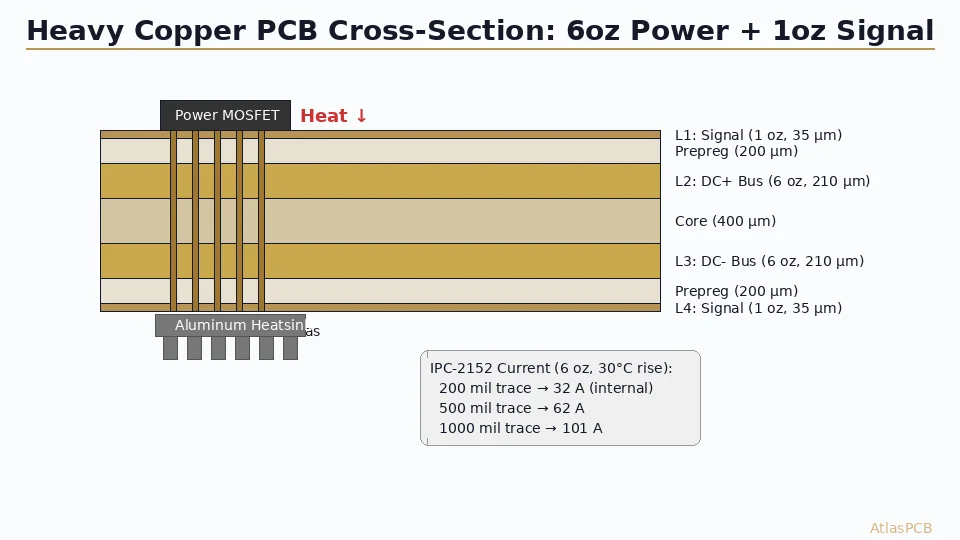
Consider a power bus requiring 30A continuous capacity. On 1oz copper with reasonable temperature rise (30C above ambient), this requires approximately 750 mil (19mm) trace width — consuming enormous board area on a single layer. Jumping to 3oz copper reduces the required width to approximately 300 mil (7.6mm), which is often practical for power electronics layouts. Alternatively, paralleling three 1oz layers each carrying 10A requires only 120 mil (3mm) width per layer.
From a cost perspective, a 6-layer 1oz board with three paralleled power layers costs roughly $14-18/board at 100-piece (100x100mm). A 4-layer board with 3oz outer copper costs $18-28/board for the same footprint. The 6-layer standard approach is often cheaper, provides better thermal spreading (three distributed heat sources vs one concentrated source), and maintains fine-pitch routing capability on signal layers. The heavy copper approach wins when board area is severely constrained or when the current path geometry requires a single wide conductor (bus bar) rather than distributed parallels.
The breakpoint typically falls around 20-25A for concentrated single-path currents. Below this threshold, multi-layer distribution is usually more cost-effective. Above it, the trace width required on 1oz copper becomes impractical regardless of layer count, making heavy copper the only viable option.
Mixed copper weight stackups offer a practical compromise. Many power electronics designs use 2oz or 3oz on the outer layers (power distribution and thermal dissipation) with 1oz on inner signal layers (maintaining fine-pitch routing). This hybrid approach costs approximately 1.4-1.6x a uniform 1oz stackup — significantly less than applying heavy copper throughout — while achieving the necessary current capacity on power distribution layers.
STACKUP OPTIMIZATION
Mixed Copper Weight Stackup? We Engineer the Optimal Solution
We routinely build mixed-weight stackups: 3oz outer for power, 1oz inner for signals. Our engineers can recommend the most cost-effective copper distribution for your current requirements.
Heavy Copper ServicesOptimization Strategies: Reducing Heavy Copper Cost Without Sacrificing Performance
The most effective cost reduction comes from avoiding heavy copper where it is not needed. Many power board designs specify uniform heavy copper across all layers “to be safe” when only specific traces or planes actually carry high current. Identifying which nets require thick copper and which can remain at 1oz or 2oz often reduces cost by 30-40% versus the uniform heavy copper approach.
Trace width optimization is the second lever. Copper thickness and trace width are interchangeable for current capacity — the IPC-2152 heating equation depends on cross-sectional area (width x thickness), not either dimension alone. If your layout has room for wider traces, you can drop copper weight and save money. A 200-mil trace at 2oz carries the same current as a 100-mil trace at 4oz, but the 2oz version costs 45% less to fabricate.
Board size directly affects heavy copper cost because fabricators charge per panel, not per unit area. If your heavy copper design is small (under 50x50mm), multiple boards fit on a single production panel, and the per-board cost drops significantly. Conversely, large heavy copper boards (200x200mm+) may only fit 2-4 per panel, making each one expensive. Optimizing board outline dimensions to maximize panel utilization can reduce unit cost by 15-25%.
Surface finish selection matters more on heavy copper boards because the increased surface area (from thicker copper edges on pads) consumes more plating chemistry. HASL is typically the most cost-effective finish for heavy copper power boards since most components are through-hole or large SMD packages that do not require the planarity of ENIG. Specifying HASL instead of ENIG on a heavy copper board saves approximately $0.50-1.50/board depending on pad count and size.
COST OPTIMIZATION
Need Heavy Copper But Watching the Budget?
Upload your design and tell us your current/thermal requirements. We will suggest the most cost-effective copper weight and stackup combination.
Compare Pricing Options ›Quantity Breakpoints and Lead Time Impact
Heavy copper boards exhibit steeper quantity discounts than standard PCBs because the setup costs (chemistry preparation, etch parameter tuning, test coupons) are fixed regardless of batch size. A single heavy copper prototype might cost $150-300 because the fabricator still needs to prepare and qualify the etch process. At 100 pieces, that same board drops to $18-28/unit as setup amortizes across production.
Lead time also increases with copper weight. Standard 1oz boards ship in 5-7 days for quick-turn orders. At 3oz, expect 7-10 days minimum because the extended etch cycles reduce daily throughput. At 5oz, 10-15 days is typical even for rush orders. The throughput bottleneck is real — a fabricator cannot simply “rush” thick copper through the etch line without risking quality. If your project timeline is tight, factor in the additional 3-7 days that heavy copper adds to standard lead times.
For prototyping, consider starting with 2oz copper even if your final production design targets 3oz or 4oz. The electrical behavior scales predictably with copper cross-section (IPC-2152 calculations), and 2oz prototypes can validate layout, thermals, and power integrity before committing to the higher cost and longer lead time of production-weight copper. Most thermal and current-capacity issues manifest at 2oz — if the board works at 2oz with acceptable margins, you have confidence that production at 3-4oz will meet spec.
ATLASPCB
Heavy Copper from Prototype to Production
We support 1oz through 5oz copper on outer layers, up to 3oz inner. Mixed-weight stackups, selective heavy copper zones, and bus-bar PCB designs. Upload your Gerber to get started.
Get Instant Quote ›
Related Reading:
About AtlasPCB — We specialize in complex PCB manufacturing for HDI, RF, and high-reliability applications. Explore our heavy copper PCB manufacturing, or get an instant online PCB quote . Every order includes free engineering review. Get your quote.
Reviewed by AtlasPCB Engineering Team — IPC-certified manufacturing specialists with 15+ years of production experience in HDI, RF, and high-reliability PCB fabrication. Content based on factory floor data and real customer design reviews.
Frequently Asked Questions
How much more does 3oz copper cost compared to 1oz on a PCB?
What minimum trace width is needed for heavy copper PCBs?
Is it cheaper to use thick copper or add layers for high-current PCBs?
Why does heavy copper PCB cost scale non-linearly with copper weight?
- heavy copper
- PCB cost
- power electronics
- pricing
- copper weight
- bus bar