· David Okafor · Engineering · 4 min read
HDI PCB Technology
Learn about HDI (High Density Interconnect) PCB technology — microvia types, laser drilling, buildup layer structures, HDI classifications, and applications in smartphones and 5G.

Quick Answer
HDI (High Density Interconnect) PCBs use microvias, laser drilling, and buildup layer structures to achieve higher wiring density than conventional PCBs. They are essential for compact electronics like smartphones, wearables, and 5G devices where standard PCB technology cannot meet density requirements.
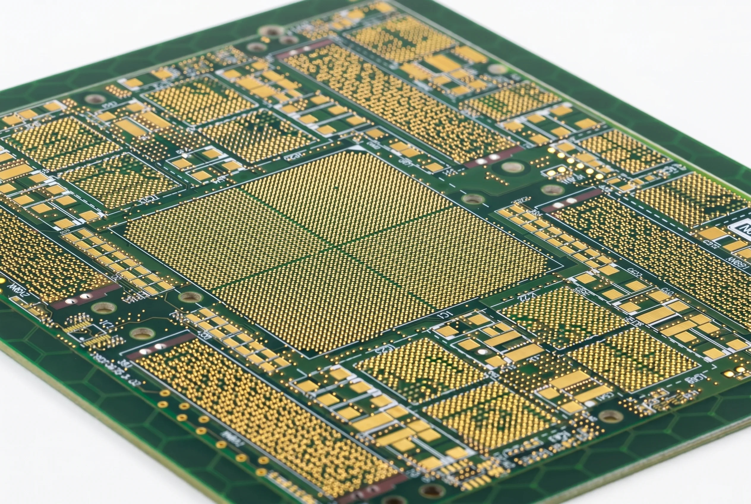
As electronic devices become smaller and more powerful, traditional PCB fabrication methods reach their limits. HDI (High Density Interconnect) technology overcomes these limitations with microvias, fine lines, and advanced buildup structures. This guide explains what HDI is, how it works, and when you need it.
What Is HDI PCB?
An HDI PCB is defined by the IPC as a board with a higher wiring density per unit area than conventional PCBs. The key distinguishing features are:
- Microvias: Holes with diameter <= 150um (6 mil), typically laser-drilled
- Fine lines: Trace width/spacing <= 75um (3 mil)
- High pad density: Via pads as small as 250um (10 mil)
- Buildup layers: Sequential lamination with one or more microvia layers
HDI vs Conventional PCB
| Feature | Conventional | HDI |
|---|---|---|
| Min via diameter | 200-300um (mechanical drill) | 75-150um (laser drill) |
| Min trace/space | 100um / 100um (4/4 mil) | 50-75um / 50-75um (2-3/2-3 mil) |
| Via pad size | 500-600um | 200-350um |
| Layer-to-layer via | Through-hole only | Microvias, blind, buried, stacked |
| BGA breakout | Limited (0.8mm+ pitch) | Full (0.3-0.4mm pitch possible) |
| Board thickness | Standard (1.0-2.0mm) | Thinner possible (0.4-1.0mm) |
HDI Buildup Structures
HDI boards are classified by the IPC into types based on their buildup structure:
Type I: 1+N+1
- One buildup layer (with microvias) on each side of an N-layer core
- Example: 1+4+1 = 6-layer board with microvias on layers 1-2 and 5-6
- Most common and cost-effective HDI type
- Sufficient for most smartphone and tablet applications
Type II: 2+N+2
- Two buildup layers on each side
- Microvias can be stacked or staggered
- Example: 2+4+2 = 8-layer board
- Required for fine-pitch BGAs (0.4mm pitch)
Type III: 3+N+3 or more
- Three or more buildup layers per side
- Features stacked microvias with copper-filled construction
- Used in the most advanced applications (high-end smartphones, advanced computing)
ELIC (Every Layer Interconnect)
- Every layer connected with microvias
- No conventional through-hole vias
- Maximum routing density
- Most expensive; used in cutting-edge designs
Microvia Technology
Laser Drilling
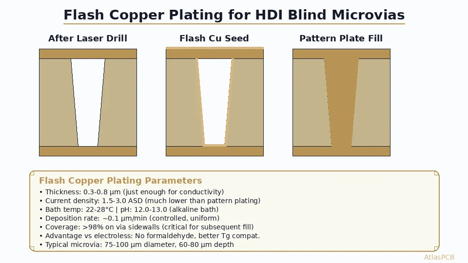
- CO2 laser: Drills through dielectric (resin + glass) to expose copper. Can’t drill through copper — requires a copper window (conformal mask) or direct ablation after copper etching.
- UV laser (Nd:YAG, 355nm): Can drill through both copper and dielectric. Smaller via diameters (25-75um) possible. Slower than CO2.
- Typical microvia: 100um diameter, 60-75um deep, drilled through one dielectric layer
Via Fill Options
- Electroplated copper fill: Vias filled with copper during plating. Required for stacked microvias. Adds cost but enables maximum density.
- Non-conductive epoxy fill: Less expensive but vias cannot be stacked directly.
- Conductive paste fill: Middle ground; used in some applications.
Stacked vs Staggered Microvias
Stacked: Microvias on consecutive layers are aligned directly on top of each other. Requires copper-filled vias for structural integrity. Highest density but highest cost.
Staggered: Microvias on consecutive layers are offset from each other. Doesn’t require copper fill. Lower cost but uses more routing space.
Design Considerations
BGA Breakout — The Primary Driver for HDI
The most common reason to use HDI is to route signals from fine-pitch BGA packages:
| BGA Pitch | Via Type Needed | HDI Type |
|---|---|---|
| 1.0mm | Standard through-hole | Not needed |
| 0.8mm | Standard or blind via | Type I (optional) |
| 0.65mm | Blind/microvia | Type I |
| 0.5mm | Microvia | Type I or II |
| 0.4mm | Stacked microvia | Type II or III |
| 0.3mm | ELIC | Type III / ELIC |
Layer Count Reduction
HDI can sometimes reduce the total layer count compared to conventional designs:
- A conventional 12-layer board might be replaced by an 8-layer HDI (2+4+2)
- Fewer layers = thinner board, lighter weight, potentially lower cost despite the HDI premium
Impedance Control in HDI
- Thinner dielectrics (50-75um vs 100-200um conventional) mean narrower traces for the same impedance
- Tight tolerance prepreg materials (RCF — Resin Coated Foil) are used for buildup layers
- Field solver simulation is essential for accurate impedance modeling
Manufacturing Process Differences
- Sequential lamination: Each buildup layer is laminated and drilled separately, unlike conventional boards where all layers are pressed at once
- Laser drilling: Replaces mechanical drilling for microvias
- Copper filling: Additional plating steps for via fill
- Tighter process controls: Registration, etching, and plating tolerances are much tighter
- Higher yield requirements: More processing steps mean more opportunities for defects
Applications
- Smartphones and tablets: Main logic boards (Apple, Samsung, etc.)
- 5G infrastructure: Antenna arrays, beamforming modules
- Wearable devices: Smartwatches, AR/VR headsets
- Automotive ADAS: Radar, lidar, camera modules
- Medical devices: Implantables, portable diagnostics
- Aerospace: Satellite systems, avionics computers
- Networking: High-speed switches, routers, server NICs
Cost Factors
| Factor | Impact on Cost |
|---|---|
| HDI type (I vs II vs III) | Each additional buildup layer +30-40% |
| Copper-filled vias | +15-25% |
| Line/space (3/3 mil vs 4/4 mil) | Tighter = +20-30% |
| Layer count | Standard pricing + HDI premium |
| Panel size utilization | Smaller boards = better utilization |
| Volume | HDI benefits significantly from volume pricing |
Typical price comparison (100x100mm, qty 10):
- 6-layer conventional: $15-25/board
- 6-layer HDI (1+4+1): $25-45/board
- 8-layer HDI (2+4+2): $45-80/board
Conclusion
HDI technology is essential for modern electronics that demand high component density, fine-pitch BGAs, and compact form factors. While more expensive than conventional PCBs, HDI can sometimes reduce overall cost by enabling fewer layers and smaller board sizes. When designing with HDI, engage your manufacturer early — their specific capabilities (laser drill size, minimum line/space, stackup options) will directly influence your design choices.
About AtlasPCB — We specialize in complex PCB manufacturing for HDI, RF, and high-reliability applications. Explore our HDI PCB manufacturing capabilities . Every order includes free engineering review. Get your quote.
Reviewed by AtlasPCB Engineering Team — IPC-certified manufacturing specialists with 15+ years of production experience in HDI, RF, and high-reliability PCB fabrication. Content based on factory floor data and real customer design reviews.
Frequently Asked Questions
What is an HDI PCB?
When do I need HDI PCB technology?
What are the main types of microvias in HDI?
- HDI
- microvia
- high density interconnect
- advanced pcb