· David Okafor · Engineering · 8 min read
Hard Gold vs ENIG for PCB Connectors
Compare hard gold (electrolytic) and ENIG surface finishes for PCB edge connectors, gold fingers, and card-edge contacts. Covers wear resistance, gold thickness, insertion cycles, cost impact, and specification guidelines for PCI Express, DDR DIMM, and industrial card-edge applications.
Quick Answer
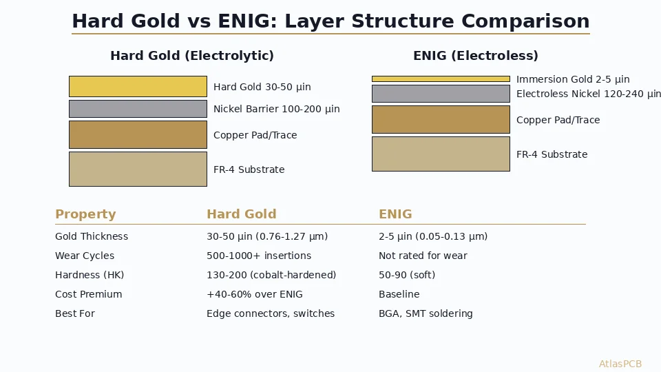
Use hard gold (30-50 µin electrolytic gold over nickel) for card-edge connectors, gold fingers, and any contact surface that will experience repeated insertion/removal cycles. Use ENIG for BGA pads, SMT soldering areas, and surfaces that only need corrosion protection without mechanical wear. Hard gold withstands 500-1000+ mating cycles; ENIG's thin immersion gold (2-5 µin) wears through in under 20 insertions.
Quick Answer: Hard Gold for Wear, ENIG for Solder
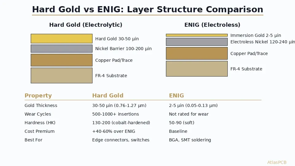
If your PCB has edge connectors, card slots, or any contact that plugs into a mating connector repeatedly, those surfaces require hard gold — period. ENIG cannot survive mechanical wear. The table below gives the engineering basis for this decision.
| Property | Hard Gold (Electrolytic) | ENIG (Electroless) |
|---|---|---|
| Gold thickness | 30-50 µin (0.76-1.27 µm) | 2-5 µin (0.05-0.13 µm) |
| Hardness | 130-200 HK (cobalt-hardened) | 50-90 HK (soft, pure gold) |
| Insertion life | 500-1000+ cycles | Not rated (< 20 cycles) |
| Contact resistance | < 20 mOhm after 500 cycles | Degrades rapidly with wear |
| Solderability | Poor (gold embrittlement risk) | Excellent (designed for solder) |
| Typical application | Card edge, gold finger, test point | BGA, QFP, SMT pads |
| Cost vs bare copper | +$2-5/board (finger area only) | +$0.50-1.00/board (full surface) |
Why Gold Thickness Matters for Connector Reliability
The fundamental difference between hard gold and ENIG comes down to a single engineering parameter: gold thickness and its mechanical hardness. When a connector mates, the contact surfaces experience both normal force (typically 50-150g per contact) and sliding displacement (0.5-2mm). This combination creates adhesive wear that progressively removes material from the contact surface with each insertion cycle.
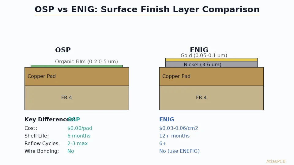
At 2-5 µin thickness, ENIG’s immersion gold functions purely as a corrosion barrier for the underlying nickel. It was never designed for mechanical contact — the gold layer exists solely to prevent nickel oxidation between PCB fabrication and soldering assembly. Under contact pressure, this thin gold layer transfers to the mating connector within the first few insertions, leaving exposed nickel that rapidly forms a resistive oxide film.
Hard gold operates in a fundamentally different regime. The electrolytic deposition process co-deposits cobalt or nickel hardening agents (0.1-0.3% by weight) within the gold matrix, increasing Knoop hardness from pure gold’s 50-70 HK to 130-200 HK. Combined with 6-25x greater thickness, the wear rate drops by orders of magnitude. A properly specified hard gold surface maintains contact resistance below 20 milliohms through 500-1000 insertion cycles — the entire useful life of most connectors.
SELECTIVE PLATING EXPERTISE
Need Hard Gold on Connectors + ENIG on SMT Pads?
We routinely produce selective-plated boards with hard gold fingers and ENIG elsewhere. Upload your Gerber with callouts and we will quote both finishes.
Upload Gerber Files ›
Specification Requirements: What to Call Out in Your Fab Drawing
Getting the plating right starts with clear communication in your fabrication drawing. Ambiguous or missing callouts are one of the most common causes of connector plating failures — the fabricator either applies the wrong finish or uses insufficient thickness because the requirement was not explicit.
For hard gold connector fingers, your fab drawing should include these specific callouts: gold thickness (minimum 30 µin per IPC-4556), nickel underplating thickness (100-200 µin), plating area boundaries (dimensioned from board edge), and any beveling requirements for card-edge insertion guidance. The bevel angle is typically 20-45 degrees and chamfers 0.5-1.0mm of the connector lip to facilitate smooth mating.
Selective plating logistics also require attention. Hard gold deposition is an electrolytic process that requires electrical current to flow through the plated surface. The fabricator routes a temporary “plating bus” — a thin copper trace connecting all gold fingers to a common rail — which is removed during final board profiling. Your design must accommodate this bus routing without violating minimum clearance rules in the connector finger area.
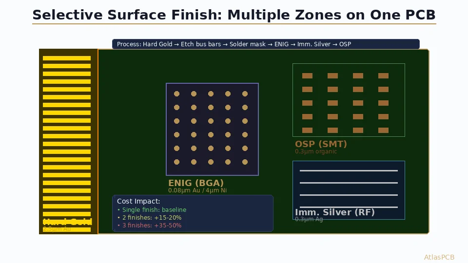
For designs requiring both hard gold and ENIG, explicitly note in the fab drawing: “Apply 30 µin minimum hard gold over 150 µin Ni to gold finger area per detail A. Apply ENIG per IPC-4552 to all other exposed copper.” This eliminates any ambiguity about which areas receive which process.
ENGINEERING REVIEW
Not Sure About Your Gold Finger Spec?
Our engineers review connector plating requirements during DFM analysis. We will flag any thickness or clearance concerns before production.
Get DFM Feedback ›Common Failure Modes and How to Avoid Them
The most expensive mistake engineers make with gold plating is using ENIG on surfaces that experience mechanical wear. This seems obvious in the context of a card-edge connector, but the same principle applies to test points that contact spring-loaded pogo pins during production testing, RF connector launch pads that mate with board-level connectors, and switch contact pads on membrane keyboards. Any surface that experiences repeated mechanical contact needs hard gold — not just formal card-edge connectors.
Gold embrittlement is the inverse failure mode: using hard gold where soldering is required. When gold dissolves into solder (which happens readily during reflow), concentrations above 3-5% by weight form brittle AuSn4 intermetallic compounds that weaken the joint. This is why you should never solder directly to hard gold surfaces — the thick gold layer provides far more gold than the solder joint can tolerate. ENIG’s thin gold layer dissolves completely and harmlessly during soldering, which is precisely its design intent.
Black pad defect affects ENIG specifically but not hard gold. The electroless nickel deposition chemistry can create hyperactive corrosion at grain boundaries, producing a dark phosphorus-rich layer that resists wetting. This affects solder joint reliability on BGA pads but is irrelevant for hard gold connector applications since those surfaces are never soldered. If your board has both connectors and fine-pitch BGAs, the combination of hard gold (fingers) plus ENEPIG (BGAs) eliminates both wear and black pad concerns — at a cost premium of roughly 25-35% over the hard gold + ENIG combination.
SURFACE FINISH OPTIONS
Hard Gold, ENIG, ENEPIG, OSP — We Do Them All
Tell us your application requirements and we will recommend the right finish combination for reliability and cost optimization.
View CapabilitiesApplication Guide: Matching Finish to Connector Type
Different connector systems have different wear requirements, and the gold thickness specification should match the expected service life rather than defaulting to maximum thickness everywhere.
PCI Express and DDR DIMM card-edge connectors typically see 20-50 insertion cycles over their lifetime (initial installation plus a few rework events). For these applications, 30 µin hard gold provides adequate margin with a safety factor of 10-20x beyond expected use. The IPC-4556 Class 1 specification covers this range and represents the most cost-effective option for consumer and commercial electronics.
Test fixtures and burn-in sockets present a more demanding environment. A production test fixture may see 50,000-100,000+ insertions per year, with spring-loaded contacts exerting higher forces than standard card-edge connectors. These applications require 50 µin minimum hard gold (IPC-4556 Class 2) and benefit from periodic contact cleaning to remove wear debris.
Industrial and military card-edge connectors specified to MIL-DTL-55302 or similar standards often require 50 µin gold with additional requirements for adhesion testing and porosity limits. The nickel underplate becomes critical here — insufficient nickel thickness (below 100 µin) allows gold porosity to create corrosion paths that undermine long-term contact reliability in harsh environments.
For RF/microwave connector launch pads (SMA, SMP, SMPM), the situation is nuanced. While these connectors mate mechanically, the contact physics differ from card-edge sliding. Many RF designs successfully use ENIG on launch pads because the connector applies primarily normal force without significant lateral sliding. However, for removable test connectors that mate/de-mate frequently during development, hard gold on the launch pad eliminates any wear concern.
ATLASPCB
Ready to Order Boards with Gold Finger Connectors?
Upload your design with connector callouts. We support selective hard gold up to 50 µin on edge connectors combined with ENIG, ENEPIG, or OSP on remaining pads.
Get Instant Quote ›
Related Reading:
About AtlasPCB — We specialize in complex PCB manufacturing for HDI, RF, and high-reliability applications. Explore our RF and high-frequency PCB services, or get an full PCB manufacturing capabilities . Every order includes free engineering review. Get your quote.
Reviewed by AtlasPCB Engineering Team — IPC-certified manufacturing specialists with 15+ years of production experience in HDI, RF, and high-reliability PCB fabrication. Content based on factory floor data and real customer design reviews.
Frequently Asked Questions
How thick should hard gold be for PCB edge connectors?
Can I use ENIG instead of hard gold on connector fingers to save cost?
What is the cost difference between hard gold and ENIG on a PCB?
Can I have both hard gold and ENIG on the same PCB?
- hard gold
- ENIG
- gold finger
- PCB connector
- edge contact
- surface finish