· Thomas Webb · Engineering · 10 min read
EV Battery Management System PCB: Bms Thermal
EV BMS PCBs operate in extreme conditions — high voltage isolation (400-800V), wide temperature range (-40C to +125C), and heavy copper for 50-200A current paths. This guide covers the PCB-specific design and manufacturing challenges for battery management systems in electric vehicles.
Quick Answer
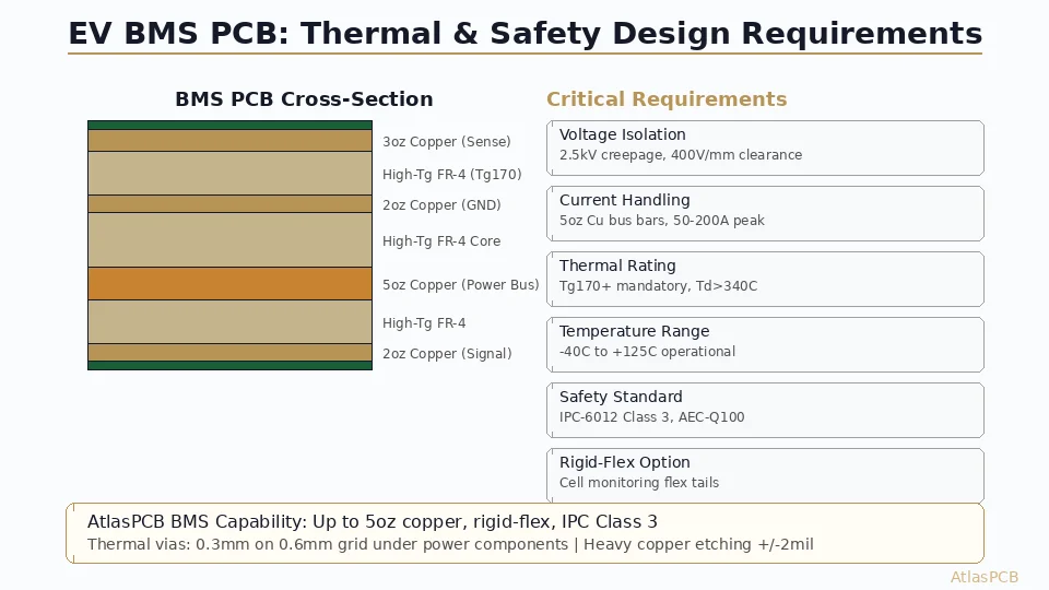
EV BMS PCBs require: 3-5oz copper on power bus layers (for 50-200A continuous current with acceptable temperature rise), high-Tg material (Tg170+ mandatory for underhood thermal cycling from -40C to +125C), minimum 2.5kV creepage/clearance isolation between high-voltage and logic sections per IPC-2221, and IPC-6012 Class 3 manufacturing to automotive reliability standards (AEC-Q100 qualification). Rigid-flex construction is increasingly common for cell monitoring connections that must withstand vibration and repeated thermal cycling without connector failures.
Quick Reference: EV BMS PCB Design Parameters
| Parameter | Specification | Standard/Source |
|---|---|---|
| Voltage isolation | 2.5kV min (400V system), 4kV (800V system) | IPC-2221, IEC 60664 |
| Creepage distance | 6.4mm (400V) / 12.5mm (800V) | IEC 60664-1, PD2 |
| Clearance distance | 4mm (400V) / 8mm (800V) | IEC 60664-1 |
| Operating temperature | -40C to +125C (underhood) | AEC-Q100 Grade 1 |
| Current capacity | 50-200A continuous on power bus | Application-specific |
| Copper weight (power layers) | 3-5oz (105-175um) | Thermal calculation |
| PCB material | FR-4, Tg >= 170C, Td >= 340C | IPC-4101 |
| Manufacturing class | IPC-6012 Class 3/A | Automotive reliability |
| Thermal cycling | 1000+ cycles, -40C to +125C | AEC-Q100 |
| Vibration | 10-2000 Hz random, 20g peak | SAE J2380 |
The EV BMS PCB is arguably the most demanding automotive PCB application because it combines high-voltage isolation, high-current thermal management, extreme temperature range, and vibration requirements simultaneously.
High-Voltage Isolation: The PCB Layout Challenge
The fundamental PCB design challenge in BMS is maintaining electrical isolation between the high-voltage battery domain (400V or 800V) and the low-voltage control/communication domain (12V/3.3V). This is not just a safety requirement — it is a regulatory necessity for vehicles sold in every major market.
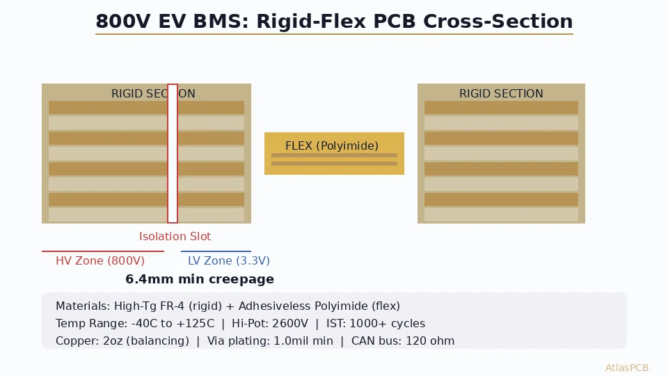
IEC 60664-1 specifies creepage and clearance distances based on working voltage, pollution degree, and insulation coordination level. For an 800V battery system with pollution degree 2 (normal automotive environment), the PCB must maintain 12.5mm minimum creepage between HV and LV sections. This distance is enormous by PCB standards — most engineers are accustomed to working with 6-8mil clearances, not 12.5mm (492mil).
The practical solution is a physical slot or cutout in the PCB between the HV and LV domains. A 2-3mm wide routed slot effectively creates infinite creepage along the slot length, requiring only the minimum clearance at the slot ends where signals must cross (via isolated gate drivers or optocouplers). In our BMS production, the typical board has a 2.5mm slot running the full length of the HV/LV boundary, with reinforced conformal coating specified around the slot edges to prevent contamination buildup that could reduce effective creepage.
The signals that cross the isolation barrier — cell voltage sense lines, communication (SPI/I2C to isolated transceiver), and fault outputs — use isolated gate drivers or capacitive/magnetic isolators that provide reinforced insulation rated to the working voltage. The PCB footprints for these components must be designed with extended creepage between input and output pin rows, typically requiring a keep-out zone that matches the 12.5mm requirement.
RIGID-FLEX PCB MANUFACTURER
EV BMS PCB Fabrication: HV Isolation + Heavy Copper
We fabricate BMS boards with up to 5oz copper, precision-routed isolation slots, and rigid-flex construction for cell monitoring. IPC-6012 Class 3 with full traceability.
Get BMS PCB Quote ›
Heavy Copper Design for High-Current Bus Bars
The power distribution paths in a BMS module carry substantial current — 50-200A continuous for main contactors, pre-charge circuits, and current sensing. At these current levels, standard 1oz (35um) copper is grossly inadequate. A 1oz copper trace would need to be over 2 inches (50mm) wide to carry 100A with acceptable temperature rise, which is impractical.
The solution is heavy copper construction: 3oz (105um) or 5oz (175um) copper weight on the power bus layers. A 5oz copper trace at 400mil (10mm) width carries 100A continuous with approximately 30C temperature rise above ambient — acceptable for underhood operation if ambient is managed. For current above 200A, embedded copper busbars (0.5-2.0mm thick copper inserts laminated into the PCB) provide even lower resistance paths.
Heavy copper fabrication introduces specific manufacturing constraints that affect the entire board design. Etching 5oz copper requires significantly more aggressive etch chemistry and longer exposure time, which causes more undercutting. The practical minimum trace/space on a 5oz layer is 8/8mil (200/200um) — far coarser than the 4/4mil achievable on standard 1oz layers. This means power layers and signal layers must be on separate copper weights, which is standard practice in BMS stackups.
In our heavy copper process, we use differential etching (different etch compensation per layer weight) and profile-controlled spray systems to maintain +/-2mil trace width accuracy on 5oz copper. Cross-section verification on every production lot confirms copper thickness uniformity across the bus bar traces — because even 10% thickness variation on a 100A path changes the temperature profile by 3-5C.
Thermal Management: Via Arrays and Material Selection
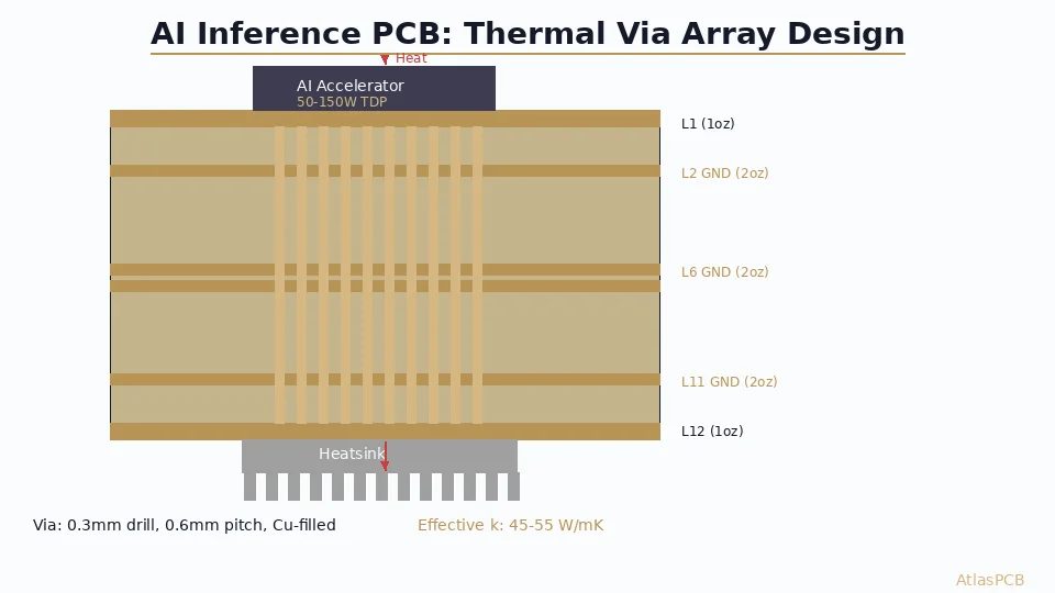
BMS PCBs dissipate significant power in MOSFETs (pre-charge, cell balancing), shunt resistors (current sensing), and isolated DC-DC converters. A typical BMS module dissipates 5-15W total, concentrated under 4-6 power components. Without proper thermal via arrays, junction temperatures exceed rated limits during continuous operation.
The thermal via design for BMS follows established principles but with tighter requirements than consumer electronics. We specify 0.3mm finished-hole-diameter vias on 0.6mm center-to-center grid pitch, filled with copper-cap resin (VIPPO process) to allow flat component mounting above the via array. This achieves thermal resistance of approximately 3-5 C/W per cm2 of via array through a 1.6mm board thickness.
Material selection directly impacts thermal reliability. Standard FR-4 (Tg130) undergoes significant Z-axis expansion above Tg — the CTE jumps from 50 ppm/C below Tg to 250+ ppm/C above Tg. In a BMS operating at 125C ambient, standard FR-4 is constantly cycling through its glass transition, accelerating via barrel fatigue. High-Tg material (Tg170, S1000-2M or equivalent) pushes this transition well above the operating temperature, maintaining stable CTE throughout the automotive temperature range.
Our standard recommendation for BMS boards is Shengyi S1000-2M (Tg170, Td350, CTE-Z 45 ppm/C below Tg). For designs requiring additional thermal margin (battery thermal runaway scenarios where localized PCB temperature may reach 200C briefly), we specify Panasonic Megtron 4 or Isola 370HR (Tg180+) on critical layers near the cell interface.
PCB MANUFACTURER FOR AEROSPACE
Automotive-Grade Thermal Reliability
We manufacture IPC-6012 Class 3 boards with verified thermal cycling reliability. Cross-section analysis, IST testing, and 100% electrical testing on every automotive lot.
Automotive PCB Capabilities ›Rigid-Flex BMS: Eliminating Connectors at the Cell Interface
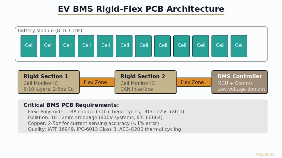
Modern BMS architectures increasingly use rigid-flex PCB construction to connect the main BMS controller board directly to cell monitoring points without intermediate wire harnesses or connectors. This trend is driven by reliability data showing that connector failures account for 23% of BMS field returns in automotive applications — primarily due to vibration-induced fretting corrosion and thermal cycling stress on crimp contacts.
A rigid-flex BMS module typically has a main rigid section containing the BMS ASIC, power electronics, and communication interfaces, with 4-12 flex tails extending to cell tap connection points. Each flex tail carries voltage sense lines (high-impedance, low-current) and thermistor connections for temperature monitoring. The flex material (polyimide, Tg > 300C) withstands the automotive thermal range without degradation, and the elimination of 12-48 connector pins per module removes the dominant failure mode.
The manufacturing challenge in rigid-flex BMS is the combination of heavy copper on the rigid section (3-5oz for power bus) and fine-line flex (1/2oz for sense lines). These require completely different etching processes on the same panel. In our facility, rigid and flex sections are processed separately through etching — the rigid section receives heavy copper etch compensation, while the flex section uses fine-line chemistry — then joined during the lamination stack. This approach avoids the compromise of trying to etch both weights simultaneously.
Vibration testing per SAE J2380 is mandatory for automotive BMS. The flex transition zones (where rigid meets flex) are the highest-stress areas. Our design rule for BMS rigid-flex requires minimum 1mm coverlay overlap into the rigid zone, no copper features within 0.5mm of the transition boundary, and stress-relief bend geometry (gradual 10:1 taper, not abrupt 90-degree transitions) at every flex entry point.
Manufacturing to Automotive Standards
EV BMS PCBs must meet IPC-6012 Class 3 (high-reliability) as a minimum, with many OEMs specifying Class 3/A (space/military addendum requirements applied to automotive applications). This is significantly more demanding than the Class 2 construction used for consumer electronics.
Key differences between Class 2 and Class 3 manufacturing that affect BMS boards: annular ring requirements increase from 1mil to 2mil minimum external (no breakout allowed), conductor width tolerance tightens from +/-20% to +/-10%, plated through-hole copper thickness increases from 0.8mil to 1.0mil minimum, and via fill quality requirements become mandatory (no more than 10% voiding in filled vias vs 25% for Class 2).
The testing regime for automotive BMS boards includes: 100% electrical test (continuity + isolation at 500V for HV sections), impedance verification on all controlled-impedance nets, microsection analysis on first-article and periodic lots (every 500 panels), IST (Interconnect Stress Testing) to validate thermal cycle reliability, and ionic cleanliness testing per IPC-TM-650 to verify contamination levels that could compromise high-voltage isolation.
From our production data, Class 3 manufacturing for BMS boards adds approximately 30-40% to the unit cost compared to equivalent Class 2 construction. The premium comes from: tighter process controls (more frequent calibration, reduced batch sizes), mandatory inspection steps (microsection every lot), higher yield fallout (5-8% more rejects due to tighter acceptance criteria), and comprehensive documentation/traceability required per IATF 16949.
IMPEDANCE CONTROLLED PCB MANUFACTURER
IPC Class 3 Manufacturing for EV Applications
We hold IPC-6012 Class 3 on all automotive PCB orders. Full traceability, microsection verification, IST testing, and 100% electrical test at rated voltage. Up to 5oz copper, rigid-flex capable.
BMS PCB Stackup Example: 8-Layer Heavy Copper Rigid-Flex
A representative stackup for a 400V BMS with integrated cell monitoring flex tails:
| Layer | Material | Weight | Function |
|---|---|---|---|
| L1 | Rigid + Flex | 2oz | Signal (isolated comm, gate drives) |
| PP | High-Tg prepreg | - | Bonding |
| L2 | Rigid only | 1oz | Ground plane (HV section) |
| Core | S1000-2M, 8mil | - | High-Tg core |
| L3 | Rigid only | 5oz | Power bus (main current path) |
| PP | High-Tg prepreg | - | Bonding |
| L4 | Rigid only | 1oz | Ground plane (LV section) |
| Core | S1000-2M, 8mil | - | High-Tg core |
| L5 | Rigid only | 1oz | LV power (12V, 3.3V rails) |
| PP | High-Tg prepreg | - | Bonding |
| L6 | Rigid only | 2oz | Signal (analog sense, SPI) |
| Core | S1000-2M, 8mil | - | High-Tg core |
| L7 | Rigid only | 1oz | Ground plane (analog reference) |
| PP | High-Tg prepreg | - | Bonding |
| L8 | Rigid + Flex | 1oz | Cell sense lines (flex tails) |
Total thickness: approximately 2.4mm (rigid section) / 0.2mm (flex tails). The 5oz L3 power bus handles the main 100A current path with sufficient width for thermal performance. HV/LV isolation is maintained by the physical slot between L3 bus bar routing domain and the LV section.
ATLASPCB
Building an EV BMS? Start with the Right PCB Partner.
EV BMS PCBs demand heavy copper, high-voltage isolation, automotive-grade reliability, and often rigid-flex construction. We combine all four capabilities in-house. Upload your BMS design for engineering review and pricing.
Get BMS PCB Quote ›
Reviewed by AtlasPCB Engineering Team — 15+ years in advanced PCB fabrication for RF, HDI, and rigid-flex applications.
Related Reading:
About AtlasPCB — We specialize in complex PCB manufacturing for HDI, RF, and high-reliability applications. Explore our rigid-flex PCB manufacturing, heavy copper PCB manufacturing, or get an aluminum and metal-core PCB services . Every order includes free engineering review. Get your quote.
Reviewed by AtlasPCB Engineering Team — IPC-certified manufacturing specialists with 15+ years of production experience in HDI, RF, and high-reliability PCB fabrication. Content based on factory floor data and real customer design reviews.
Frequently Asked Questions
What copper weight is needed for EV BMS power bus PCBs?
Why is rigid-flex used in BMS designs?
What PCB material is specified for automotive BMS under-hood applications?
What creepage and clearance distances are required for 400V/800V BMS PCBs?
How does AtlasPCB handle the thermal via requirements for BMS power sections?
- EV BMS PCB
- rigid-flex PCB manufacturer
- automotive PCB
- heavy copper PCB
- thermal management PCB