· Dr. Chen Wei · Engineering · 4 min read
EMC/EMI Design for PCBs
Practical EMC/EMI design techniques for PCBs — understand radiated and conducted emissions, filtering, shielding, grounding, and layout strategies to pass FCC, CE, and CISPR compliance testing.

Quick Answer
EMC/EMI PCB design minimizes electromagnetic interference through proper grounding, shielding, filtering, and layout techniques. Key practices include continuous ground planes, short return paths, component placement to minimize loop area, and controlled impedance for high-speed signals.
EMC (Electromagnetic Compatibility) compliance is a legal requirement for selling electronic products in most markets. Failing EMC testing can delay product launch by weeks or months. This guide covers practical PCB-level techniques to pass EMC testing on the first attempt.
EMC Fundamentals
Emissions vs Immunity
- Emissions: Electromagnetic energy your product radiates (radiated) or conducts (conducted) that could interfere with other devices
- Immunity: Your product’s ability to operate correctly when exposed to external electromagnetic interference
Key Standards
| Standard | Region | Type | Frequency Range |
|---|---|---|---|
| FCC Part 15 | USA | Emissions | 30 MHz - 40 GHz |
| EN 55032 (CISPR 32) | EU | Emissions | 150 kHz - 6 GHz |
| EN 55035 (CISPR 35) | EU | Immunity | Various |
| EN 61000-4-x | EU | Immunity tests | ESD, surge, EFT, etc. |
Class A vs Class B
- Class A (Industrial): Less stringent emission limits. For equipment used in industrial/commercial environments.
- Class B (Residential): Stricter limits (~10dB lower). For equipment used in residential environments. Most consumer products must meet Class B.
PCB-Level EMI Sources
Clock Signals
- Strongest narrowband emission sources (harmonics of the fundamental frequency)
- A 100 MHz clock has significant harmonics at 300, 500, 700, 900 MHz
- Even duty cycle asymmetry of 1% creates strong even harmonics
High-Speed Data Buses
- DDR, PCIe, USB, HDMI — broadband emission sources
- Signal edge rate determines the emission bandwidth (faster edges = higher frequency content)
Power Supply Switching
- Switch-mode converters generate conducted and radiated emissions at switching frequency and harmonics
- Typical range: 100 kHz - 30 MHz
I/O Cables
- Cables act as antennas — they radiate common-mode noise picked up from the PCB
- Cable length approaching lambda/4 at a noise frequency = efficient antenna
PCB Design Techniques for EMC
1. Layer Stackup
- Ground plane adjacent to every signal layer
- Signal-ground-signal-ground ordering
- Power and ground planes adjacent for maximum decoupling
- Keep high-speed signals as striplines (between two ground planes)
2. Return Path Management
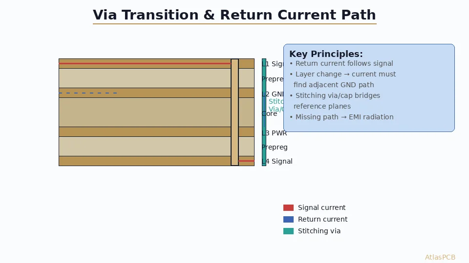
- Never route signals across ground plane gaps
- When changing signal layers, place a ground via near the signal via
- Clock signals should have dedicated return paths (ground guard traces)
3. Decoupling
- 0.1uF + 1uF per IC power pin minimum
- Capacitors as close to pins as possible (<2mm)
- Use low-ESL packages (0402 or smaller, reverse geometry)
- Bulk capacitors (10-100uF) near power entry points
4. Filtering
- Pi filters on power supply outputs (L-C-L or C-L-C)
- Common-mode chokes on I/O lines (USB, Ethernet, HDMI)
- Ferrite beads on power supply rails to isolate sections
- RC/LC filters on clock outputs to slow edge rates
5. I/O Connector Area Design
- Ground plane continuous up to connector pins
- Filter components placed at the connector, before signals enter the board
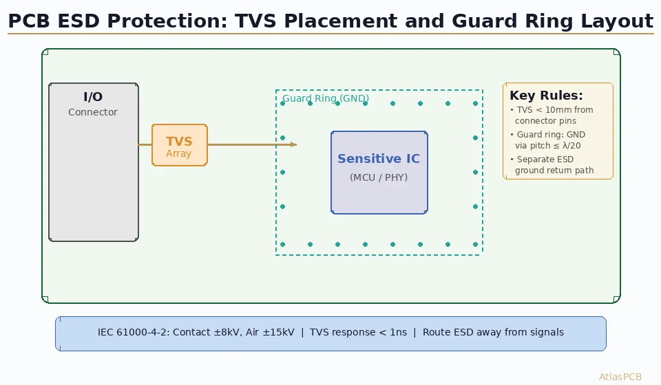
- ESD protection (TVS diodes) at every external I/O
- Ground stitching vias around connector footprint
6. Board Edge Design
- No high-speed traces near board edges (minimum 3x trace width from edge)
- Ground pour to board edge on all layers
- Via stitching along all board edges
- No signal traces or power traces on outermost 2mm
7. Shield Can Integration
- Design footprint and mounting pads for EMI shield cans
- Ground connection around full perimeter (every 2-3mm)
- Shield can grounding wall vias in the PCB
- Plan for shield can early — adding later is expensive
Conducted Emissions Reduction
Power Line Filtering
- Common-mode choke at power input (blocks CM noise from leaving via power cable)
- X capacitors (line-to-line) for differential mode noise
- Y capacitors (line-to-ground) for common-mode noise
- Pi filter topology: Y-cap → CM choke → Y-cap
Switching Power Supply Layout
- Minimize current loop area in the switch node
- Keep switch node trace short and wide
- Input capacitor as close to MOSFET as possible
- Shield the inductor or use shielded inductors
- Snubber circuit to reduce ringing
Pre-Compliance Testing
Before going to a test lab, perform pre-compliance measurements:
Near-Field Probing
- Use H-field and E-field probes with a spectrum analyzer
- Identify hot spots on the board
- Measure before and after design changes
Conducted Emissions Measurement
- LISN (Line Impedance Stabilization Network) + spectrum analyzer
- Quick measurement of power line noise
- Identifies frequency peaks for targeted filtering
Conclusion
EMC compliance starts at the PCB design stage, not at the test lab. A solid ground plane, proper decoupling, careful signal routing, and I/O filtering address 80% of EMC issues. The remaining 20% requires targeted solutions based on pre-compliance measurements. Budget time and cost for EMC design review, pre-compliance testing, and at least one design iteration. The cost of EMC-aware design from the start is far less than the cost of redesigning a non-compliant product.
Further Reading
[PCB Grounding Techniques: Star, Split, and Solid Ground Plane Strategies]/blog/pcb-grounding-techniques/)
[HDI PCB Design Guide: Stackup Rules, Via Structures & DFM Checklist]/blog/hdi-pcb-design-guide/)
[PCB Manufacturer with Engineering Review: Why Human DFM Audit Matters]/blog/pcb-manufacturer-engineering-review/)
About AtlasPCB — We specialize in complex PCB manufacturing for HDI, RF, and high-reliability applications. Explore our impedance-controlled PCB manufacturing . Every order includes free engineering review. Get your quote.
Reviewed by AtlasPCB Engineering Team — IPC-certified manufacturing specialists with 15+ years of production experience in HDI, RF, and high-reliability PCB fabrication. Content based on factory floor data and real customer design reviews.
Frequently Asked Questions
How do I reduce EMI in PCB design?
What is the difference between EMI and EMC?
- EMC
- EMI
- compliance
- pcb design