· Sophia Reyes · Engineering · 7 min read
Edge AI PCB Design
Explore the unique PCB design challenges of edge AI hardware — from thermal via arrays managing 25W NPU chips in constrained form factors to DDR5/LPDDR5X routing and multi-rail power delivery networks for 45-80 TOPS AI accelerators.
Quick Answer
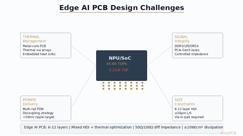
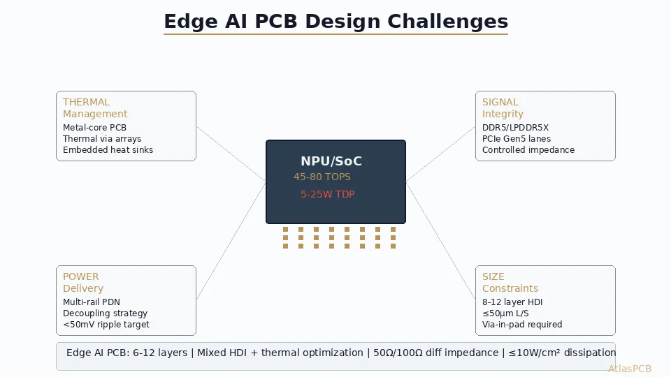
Edge AI PCB design requires solving four simultaneous challenges: thermal management for 5-25W NPUs in compact enclosures (using thermal via arrays, metal-core substrates, and embedded heat sinks), high-speed signal integrity for DDR5/LPDDR5X and PCIe Gen5 interfaces, low-noise multi-rail power delivery with <50mV ripple, and aggressive miniaturization using 8-12 layer HDI with ≤50μm trace/space.
The Edge AI Hardware Revolution
Edge AI is no longer a concept — it’s shipping in volume. From automotive ADAS cameras and industrial quality inspection systems to smart home devices and wearable health monitors, AI inference is moving to the point of data generation. The Wevolver Edge AI Report 2026, published in collaboration with Siemens, Qualcomm, and industry contributors, identifies PCB-level design as a critical bottleneck in the deployment pipeline.
The numbers tell the story: Qualcomm’s Snapdragon X Elite delivers 45 TOPS, AMD’s Ryzen AI 300 pushes 50-80 TOPS, and specialized accelerators like Hailo-10 achieve 40 TOPS in under 3W. These processors demand PCB substrates that simultaneously manage heat, maintain signal fidelity, deliver clean power, and fit in palm-sized enclosures.
Challenge 1: Thermal Management in Constrained Form Factors
The Problem
Edge AI devices don’t have the luxury of server-class cooling. A 15W NPU in a 50×50 mm board area with a sealed enclosure must dissipate heat through the PCB itself and a small heatsink — no fans, no liquid cooling, no airflow.
Traditional embedded designs dissipated 1-3W. Edge AI processors push 5-25W in similar form factors, creating thermal flux densities of 5-15 W/cm² that can cause:
- Junction temperature exceeding safe operating limits (105-125°C)
- Thermal throttling that reduces inference throughput by 30-50%
- Solder joint fatigue from thermal cycling
- Adjacent component reliability degradation
PCB-Level Thermal Solutions
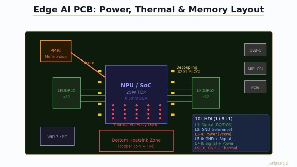
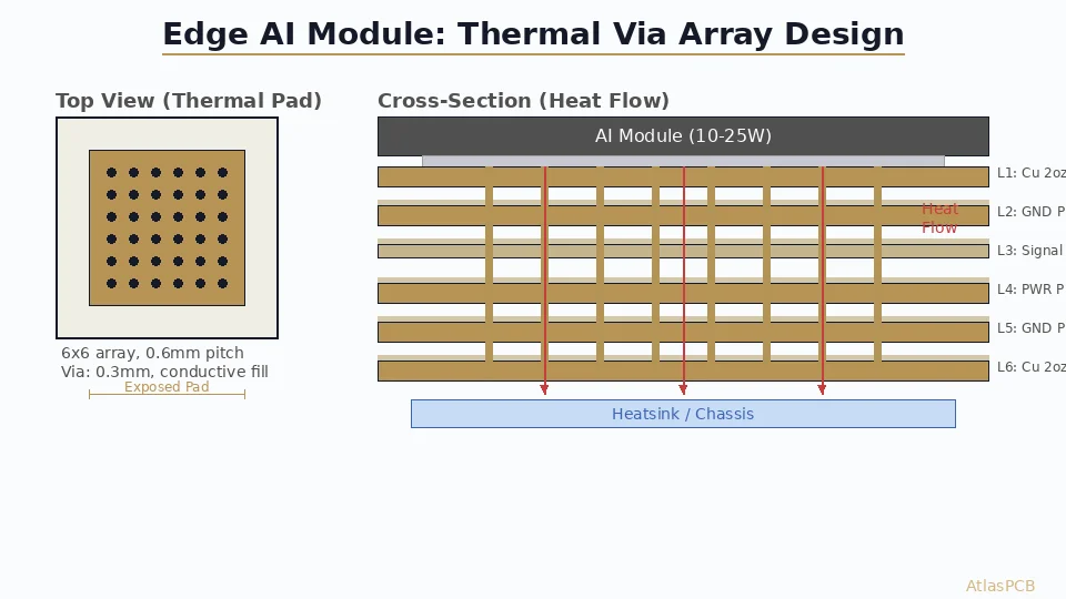
Thermal via arrays:
- Place under exposed thermal pad of NPU
- Grid pattern: 0.3 mm drill, 1.0 mm pitch (or 0.25 mm drill, 0.8 mm pitch for HDI)
- Filled with copper or conductive epoxy (not air-filled — eliminates voiding during reflow)
- Connect to internal copper planes for lateral heat spreading
- Effective thermal conductivity improvement: 3-5× vs bare FR-4
Heavy copper inner layers:
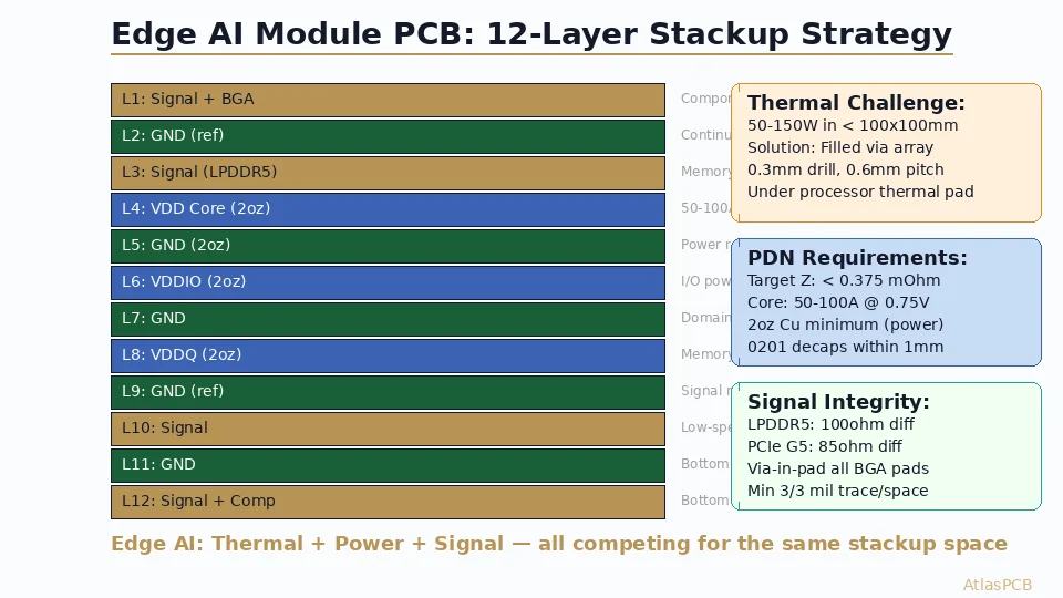
- 2 oz (70 μm) minimum on planes adjacent to NPU
- 4 oz (140 μm) for designs exceeding 20W without active cooling
- Copper-filled via connections between heavy copper layers
- Trade-off: heavier copper limits fine-pitch routing capability
Metal-core PCB (MCPCB) regions:
- Aluminum or copper core directly under high-power components
- Thermal conductivity: 1-4 W/mK (aluminum) vs 0.3 W/mK (FR-4)
- Hybrid approach: metal-core in power/thermal zone, standard HDI in signal zone
- Suitable for designs exceeding 30W total dissipation
Embedded heat sinks:
- Copper coins (2-5 mm thick) embedded in PCB stackup
- Direct thermal path from chip pad to heatsink mounting surface
- Requires special fabrication: cavity milling → coin insertion → lamination
- Achieves thermal resistance <1°C/W from die to ambient
Thermal Simulation Requirements
For edge AI designs, thermal simulation is mandatory — not optional:
- Steady-state analysis: Verify junction temperature under maximum sustained inference load
- Transient analysis: Model burst workloads (10-30 second inference cycles with idle periods)
- PCB contribution: Model copper percentage on each layer to calculate effective in-plane thermal conductivity
- Enclosure interaction: Include housing, gaskets, and environmental temperature in boundary conditions
Designing Edge AI Hardware? Talk to Our Thermal Experts.
AtlasPCB specializes in thermal-optimized PCBs: heavy copper, embedded heat sinks, metal-core hybrids, and thermal via arrays. Free thermal DFM review with every quote.
Get Thermal PCB Quote →Challenge 2: Signal Integrity for AI Memory and Interconnects
High-Speed Interfaces on Edge AI Boards
Edge AI processors communicate with their memories and peripherals through increasingly demanding interfaces:
| Interface | Data Rate | Impedance | Routing Challenge |
|---|---|---|---|
| LPDDR5X | 8533 MT/s | 40/80 Ω | Tight length matching (±2 ps) |
| DDR5 | 6400-8800 MT/s | 40/80 Ω | Fly-by topology, write leveling |
| PCIe Gen5 | 32 GT/s | 85/170 Ω | <4 dB insertion loss budget |
| MIPI CSI-2 (camera) | 4.5 Gbps/lane | 100 Ω diff | Controlled impedance, EMI control |
| USB4 | 40 Gbps | 85 Ω | Ultra-short stub lengths |
DDR5/LPDDR5X Routing on Compact Boards
Memory routing for edge AI is uniquely challenging because:
- Limited escape room: LPDDR5X packages use 0.4-0.5 mm pitch BGA, requiring via-in-pad on every signal
- Length matching tolerance: ±2 ps within a byte group (approximately ±0.3 mm in FR-4)
- Noise sensitivity: AI inference creates bursty memory access patterns with rapid current transitions
- Stack-up constraints: Data signals need solid reference planes directly adjacent (no ground plane sharing)
Best practices for edge AI memory routing:
- Route all DDR5 signals on the same layer pair (adjacent to unbroken ground)
- Use 50 μm trace/space for 0.4 mm BGA escape
- Minimize via stubs — use blind vias or back-drill for signals >6400 MT/s
- Place decoupling capacitors within 1 mm of each power/VTT pin
- Keep VREF routing away from switching signals (separate layer or heavy shielding)
PCIe Gen5 in Compact Form Factors
PCIe Gen5 at 32 GT/s has a total channel insertion loss budget of approximately 28 dB. In edge AI designs where the link may be short (20-50 mm), the challenge shifts from length to:
- Via transitions (each via pair costs 1-3 dB)
- Connector contacts (if using M.2 or card-edge)
- Reference plane discontinuities
- Impedance variations from HDI layer thickness tolerance (±10%)
Challenge 3: Multi-Rail Power Delivery Network
Edge AI Power Architecture Complexity
A typical edge AI SoC requires 5-8 separate voltage rails:
| Rail | Voltage | Current | Function |
|---|---|---|---|
| VDD_CORE | 0.7-0.85V | 5-15A | NPU/GPU core |
| VDD_SRAM | 0.75V | 1-3A | On-chip SRAM |
| VDDQ (DDR) | 1.1V | 2-5A | Memory I/O |
| VDD_IO | 1.8V / 3.3V | 0.5-2A | General I/O |
| VDD_PLL | 0.9V | 0.1-0.3A | PLL (ultra-low noise) |
| VDD_ANA | 1.2V | 0.2-0.5A | Analog/ADC |
Dynamic Load Challenge
The defining characteristic of AI workload power delivery: extreme transient current demand. An NPU switching from idle to full inference in <1 μs creates:
- di/dt: 10-50 A/μs current slew rates
- Voltage droop: Without adequate decoupling, >100 mV undershoot
- Target: Keep ripple <50 mV on 0.8V rail (6.25% tolerance)
- Required PDN impedance: <5 mΩ from DC to 100 MHz
PCB-Level PDN Optimization
- Dedicated power planes: One full copper plane per major rail (VDD_CORE must have unbroken pour)
- Distributed decoupling: 100-200 capacitors per rail, placed in concentric rings:
- 0201 MLCC (100 nF): Within 0.5 mm of BGA pads
- 0402 MLCC (1-10 μF): Within 2 mm
- Bulk electrolytic (47-100 μF): Within 10 mm
- Low-inductance power vias: Use multiple vias per power connection (4-8 vias per BGA power ball)
- Minimize anti-pad disruption: Keep signal via anti-pads small to preserve power plane continuity
- Separate analog and digital grounds: Connect at a single point near ADC reference
Challenge 4: Miniaturization and HDI Requirements
Typical Edge AI Board Parameters
| Feature | Requirement |
|---|---|
| Board dimensions | 30×30 mm to 80×100 mm |
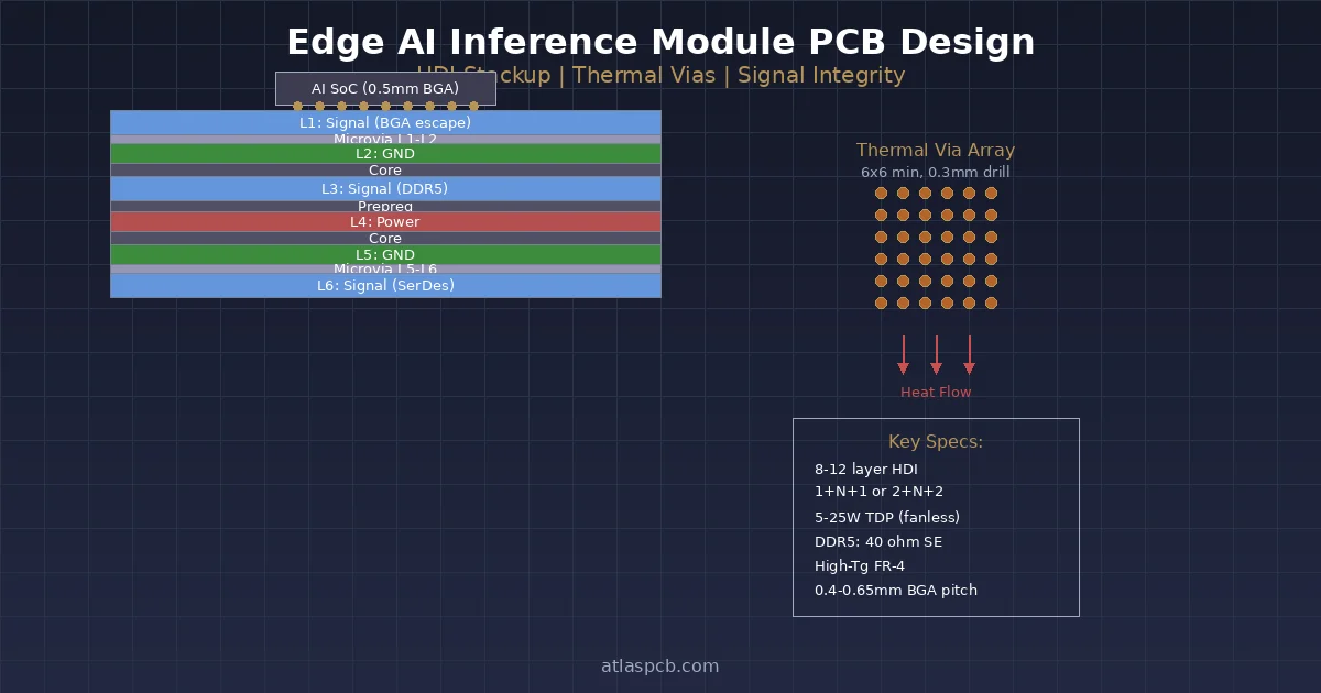
| Layer count | 8-12 layers |
| HDI configuration | 2+N+2 or 3+N+3 |
| Min trace/space | 50/50 μm (advanced: 30/30 μm) |
| Via technology | Stacked microvias, copper-filled |
| BGA pitch | 0.4-0.65 mm |
| Component density | 30-50 components/cm² |
Design Strategies for Maximum Density
- Via-in-pad everywhere: Eliminate dog-bone fanout to save 40% routing area
- Stacked microvias: 3-high copper-filled stacks for BGA escape through multiple layers
- Embedded passives: Embedded capacitors in laminate reduce surface component count
- Back-side components: Place decoupling caps on bottom directly under NPU BGA
- Component-free keep-out zones: Minimize thermal pad area wasted by clearance rules
Material Selection for Edge AI
Recommended Laminates
| Application Tier | Material | Properties | Use Case |
|---|---|---|---|
| Standard | High-Tg FR-4 (Tg 170°C) | Dk 4.2, Df 0.02 | ≤6400 MT/s DDR5 |
| Performance | Megtron 4 / EM-370 | Dk 3.8, Df 0.008 | PCIe Gen5, 8800 MT/s |
| High-end | Megtron 6 / TU-872 | Dk 3.4, Df 0.004 | PCIe Gen6, 112G SerDes |
| Thermal | Metal-core hybrid | TC 1-4 W/mK | >20W without heatsink |
Build-Up Film Selection
For the microvia build-up layers:
- ABF GX-92: Standard, good laser drilling, Dk 3.3
- ABF GZ-41: Low-loss variant, Dk 3.0, Df 0.003 — suitable for high-speed edge AI
- Panasonic R-1515V: Alternative with excellent microvia reliability
Design Workflow Recommendations
- Start with thermal analysis — Determine required copper weight and cooling strategy before stackup
- Lock memory topology early — DDR5/LPDDR5X routing drives layer count and stackup
- Simulate PDN impedance — Verify Z_target is achievable with proposed stackup
- Iterate stackup with fabricator — Edge AI stackups often push limits; verify DFM early
- Plan for yield — Fine-feature HDI has lower yield; factor into BOM cost
Further Reading
- PCB Thermal Via Array Design Rules
- AI Hardware PCB Thermal Management: Multilayer Design
- Any-Layer HDI PCB Design for Wearables and SiP
- Controlled Impedance PCB Design and Stackup Calculations
Build Your Edge AI Hardware with AtlasPCB
Edge AI PCB design pushes every manufacturing capability to its limit — thermal management, fine-feature HDI, controlled impedance, and power plane integrity all on the same 8-12 layer board. AtlasPCB’s advanced manufacturing platform handles the full spectrum: any-layer microvias, heavy copper (up to 4 oz), thermal via arrays, and 50/50 μm trace/space with IPC Class 3 quality.
About AtlasPCB — We specialize in complex PCB manufacturing for HDI, RF, and high-reliability applications. Explore our HDI PCB manufacturing capabilities, impedance-controlled PCB manufacturing, or get an aluminum and metal-core PCB services . Every order includes free engineering review. Get your quote.
Reviewed by AtlasPCB Engineering Team — IPC-certified manufacturing specialists with 15+ years of production experience in HDI, RF, and high-reliability PCB fabrication. Content based on factory floor data and real customer design reviews.
Frequently Asked Questions
What PCB layer count is needed for edge AI designs with NPU processors?
How do you manage thermal dissipation for edge AI NPUs on small PCBs?
What makes power delivery harder for edge AI compared to traditional embedded designs?
- edge ai
- npu
- pcb design
- thermal management
- signal integrity
- power delivery
- hdi
- ai hardware