· Sophia Reyes · Engineering · 6 min read
Differential Pair Routing
A complete guide to differential pair routing on PCBs — covering impedance targets, trace geometry, length matching, via transitions, common mistakes, and stackup considerations for USB, PCIe, HDMI, and Ethernet designs.
Quick Answer
Differential pair routing uses two complementary signal traces (D+ and D−) that carry equal-and-opposite signals, providing superior noise immunity and EMI performance for high-speed interfaces. The key design parameters are: differential impedance (typically 90Ω or 100Ω depending on the interface standard), trace width, gap spacing, and dielectric thickness — all of which must be calculated together using a field solver or impedance calculator. Critical routing rules include maintaining constant spacing between the pair, length matching within ±5 mil (±127μm) for most protocols, avoiding reference plane breaks, and using symmetric via transitions. Proper differential pair routing enables reliable data transfer at speeds from USB 2.0 (480 Mbps) through PCIe 5.0 (32 GT/s) and beyond.
Every high-speed interface in modern electronics — USB, PCIe, HDMI, Ethernet, SATA — relies on differential signaling. Two traces, equal and opposite signals, one clean data link. The concept is simple. Getting the routing right is where most boards fail.
This guide covers the geometry, the impedance math, the routing rules, and the mistakes that will cost you a respin.
How Differential Pairs Work
A differential pair consists of two traces — conventionally called D+ and D− (or P and N). The transmitter drives equal-and-opposite voltages on each trace. The receiver reads only the difference between them.
Why this matters: Noise from power supplies, adjacent traces, and external EMI couples equally into both traces. When the receiver subtracts D− from D+, the common-mode noise cancels. This is why differential signaling dominates above ~100 MHz.
Impedance Targets by Interface
Every differential interface specifies a target impedance. Your trace geometry must hit this target within tolerance, or the signal reflects at impedance discontinuities and corrupts data.
Notice the pattern: As data rates increase, skew tolerance gets dramatically tighter. USB 2.0 allows ±150 mil; USB 3.x allows only ±5 mil. That is a 30× tighter requirement, which fundamentally changes how you route.
Trace Geometry: Width, Gap, and Stackup
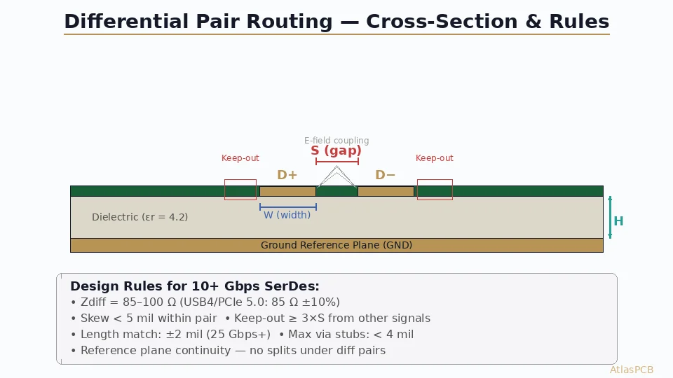
Differential impedance is determined by four variables working together. You cannot set them independently.
The Relationship
For edge-coupled microstrip (outer layer routing):
- Wider traces (W↑) → lower impedance
- Wider gap (S↑) → higher impedance (less coupling)
- Thicker dielectric (H↑) → higher impedance
- Higher Dk material → lower impedance
Typical Geometries
For standard 4-layer FR4 (Dk ≈ 4.3, dielectric ≈ 4-5 mil to plane):
| Target Zdiff | Trace Width (W) | Gap (S) | Dielectric (H) |
|---|---|---|---|
| 90Ω (USB) | 4.5–5.5 mil | 4–6 mil | 4–5 mil |
| 100Ω (HDMI/Ethernet) | 4.0–5.0 mil | 5–8 mil | 4–5 mil |
| 85Ω (PCIe) | 5.0–6.0 mil | 4–5 mil | 4–5 mil |
Always use a field solver or your manufacturer’s impedance calculator. These values are starting points — actual results depend on your specific stackup, copper weight, and solder mask effects.
Routing Rules
Rule 1: Maintain Constant Spacing
The gap between D+ and D− must stay constant along the entire route. Any gap change causes a local impedance discontinuity.
Rule 2: Length Match Within the Pair
D+ and D− must be the same electrical length. Any mismatch converts differential signal to common-mode noise, degrading eye pattern and increasing jitter.
Use serpentine (accordion) tuning on the shorter trace, placed as close to the source of mismatch as possible. Keep serpentine amplitude small — just enough to compensate.
Rule 3: No Reference Plane Breaks
Differential pairs must have a continuous reference plane (GND or power) directly below them. Slots, splits, or gaps in the reference plane under a differential pair cause:
- Impedance spike at the break
- Return current forced to find alternate path
- Increased EMI radiation from the gap
If you must cross a plane split, route the pair perpendicular to the split to minimize exposure, and add stitching vias on both sides.
Rule 4: Symmetric Via Transitions
When transitioning between layers, both traces must use identical via structures:
- Same via size and pad diameter
- Same distance from pad to trace
- Matching ground return vias adjacent to the signal pair
- GND vias placed symmetrically — one on each side, equidistant
Rule 5: Isolation from Other Signals
Keep differential pairs isolated from single-ended signals and other pairs:
- Minimum 3× gap distance from other traces (3S rule)
- Guard traces with ground vias for critical high-speed pairs
- Avoid parallel routing with other signals for more than 1 inch
Common Mistakes
Stackup Recommendations
Differential pair performance depends heavily on the PCB stackup. Here are practical guidelines:
4-layer board — Route pairs on the outer layers (L1/L4) with dedicated GND planes on L2 and L3. This gives tight dielectric control and clean reference planes.
6-layer board — Use L1 and L6 for component-side pairs, L3/L4 as inner routing layers for less critical pairs, with GND on L2 and L5. Keeps pairs close to their reference planes.
8+ layer board — Dedicate specific layers for high-speed differential routing. Adjacent ground planes on both sides (stripline configuration) provide the best impedance control and shielding.
The key principle: Every differential pair needs a solid, unbroken reference plane on the immediately adjacent layer. This is non-negotiable.
Manufacturer Considerations
When sending your design for fabrication, communicate clearly:
- Specify impedance targets — call out Zdiff for each pair class in your fab notes
- Provide the stackup — do not let the manufacturer guess. Specify layer order, dielectric thickness, and materials
- Request impedance test coupons — TDR (Time Domain Reflectometry) coupons on the panel edge verify that the manufacturer hit your targets
- Review Dk values — confirm the actual Dk of the laminate at your signal frequency, not just the datasheet nominal value
At AtlasPCB, our engineering pre-audit includes impedance stackup verification. We run your target impedance through our field solver against the proposed stackup and flag any geometry changes needed — before production begins.
Key Takeaways
Differential impedance is a system property — W, S, H, and Dk must be solved together, not set independently
Constant gap spacing is the #1 rule — any gap change is an impedance discontinuity
Length matching tightens dramatically with speed — USB 3.x needs 30× tighter matching than USB 2.0
Unbroken reference plane under every pair — no exceptions, no compromises
Always use a field solver for final impedance calculations — rules of thumb fail at high speeds
Communicate impedance specs to your manufacturer in fab notes and request TDR test coupons
Designing a board with high-speed differential pairs? Upload your Gerber files for a free impedance stackup review, or talk to an engineer about your signal integrity requirements.
Further Reading
[HDI PCB Design Guide: Stackup Rules, Via Structures & DFM Checklist]/blog/hdi-pcb-design-guide/)
[HDI PCB Technology: Microvias, Laser Drilling, and High-Density Design]/blog/hdi-pcb-technology/)
[Impedance Controlled PCB Manufacturer: ±5% Guaranteed with TDR Testing]/blog/impedance-controlled-pcb-manufacturer/)
[High-Speed PCB Design: Signal Integrity Essentials for Modern Electronics]/blog/high-speed-pcb-design/)
[PCB Gerber Files: What They Are and How to Generate Them]/blog/pcb-gerber-files-guide/)
[PCB Solder Mask: Types, Colors, and Functions Explained]/blog/pcb-solder-mask-guide/)
[IPC Class 3 Requirements: The Complete Guide for Designers]/blog/ipc-class-3-requirements/)
[EMC/EMI Design for PCBs: Passing Compliance on the First Try]/blog/emc-emi-pcb-design/)
About AtlasPCB — We specialize in complex PCB manufacturing for HDI, RF, and high-reliability applications. Explore our impedance-controlled PCB manufacturing, or get an Megtron 6 & 7 low-loss PCB manufacturing . Every order includes free engineering review. Get your quote.
Reviewed by AtlasPCB Engineering Team — IPC-certified manufacturing specialists with 15+ years of production experience in HDI, RF, and high-reliability PCB fabrication. Content based on factory floor data and real customer design reviews.
Frequently Asked Questions
What is differential pair routing in PCB design?
What is the standard differential impedance for USB and PCIe?
How tight does length matching need to be for differential pairs?
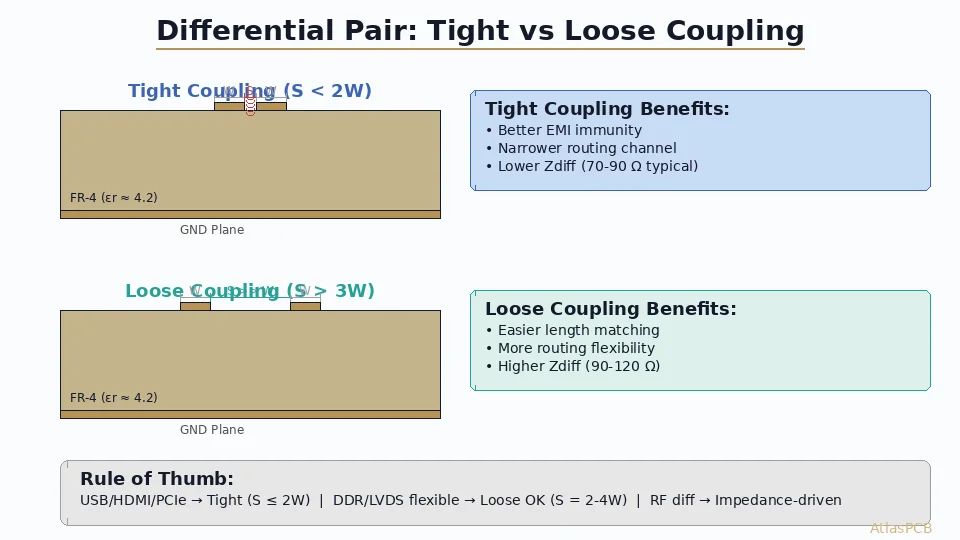
Should differential pairs be tightly or loosely coupled?
- differential pair
- signal integrity
- impedance control
- high speed pcb
- pcb routing
- pcb design